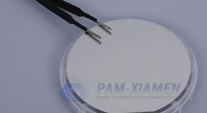
GaInP / AlInP Light Emitting Diode Structure
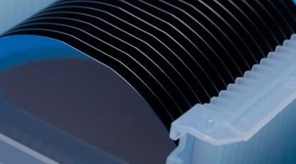
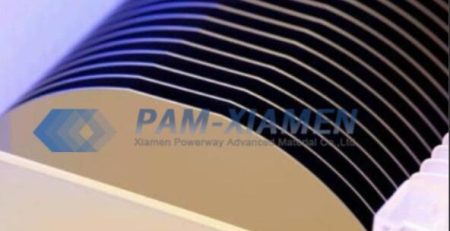
Light emitting diode (LED) structure with GaInP / AlInP epilayers can be offered by Ganwafer. The ternary InGaP and AlInP materials are lattice matched to GaAs susbtrate, which can be grown by MOCVD. Growing high quality III-V ternary semiconductor material is important to the fabrication of light emitting diodes, laser diodes and multi-junction photovoltaic. Light emitting diode structure with ternary GaInP and AlInP epilayers from Ganwafer is shown as follows:
1. GaAs Epi Structure of Light Emitting Diode
No.1 GaAs LED Epitaxy
|
GaAs LED Structure (GANWP20065-LED) |
||
| Layer Material | Thickness | Note |
| p-GaInP | – | Composition of In: 0.5;
Mg doped |
| p-GaP | – | |
| p-AlInP | – | |
| MQW | – | |
| n-AlInP | – | |
| DBR | – | |
| Etch stop n-GaInP | 20 nm | |
| Buffer layer | – | |
| GaAs subs. | 350 um | |
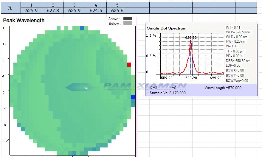
PL and El test of quantum light emitting diode wafer is shown as the diagram:
No. 2 GaAs based InGaP LED Epitaxy Wafer
GANW190724-INGAP
| Layer Name | Material | Thickness |
| P-cladding layer | P-AlInP | – |
| Active layer | MQW | – |
| N-cladding layer | N-AlInP | 900nm |
| Bragg reflector | N-AlGaAs/AlAs | – |
| Buffer layer | N-GaAs | |
| Substrate | N-GaAs on-axis (100) plane without offcut |
No. 3 GaAs based LED Epitaxial Structure
GANWP19168-INGAP
| Layer Name | Material | Thickness |
| P-cladding layer | P-AlInP | – |
| Active layer | MQW | – |
| N-cladding layer | N-AlInP | – |
| Buffer layer | N-GaAs | 300nm |
| Substrate | N-GaAs on-axis (100) plane without offcut |
2. FAQ of GaAs Light Emitting Diode Wafer
Q:We observed two MQW regions in GaInP LED wafer (GANWP19168-INGAP), illustrated in below figure. There are 9 pairs in each MQW separated by a thick barrier layer. May I know any reason to grow this kind of structure instead of a single stack of MQWs?
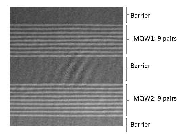
A: These are two groups of identical quantum wells in InGaP LED epitaxy. In order to increase the thickness of the active region and improve the reliability of the LED chip, the middle layer can be used normally without any influence on the photoelectric performance.
3. InGaP on GaAs for Light Emitting Diode Structure
InGaP, which shows great potential to substitute the aluminum contained materials, is a critical semiconductor material usually grown on GaAs substrate. Its properties are closely related to growth conditions, such as growth method, substrate temperature, growth rate, substrate orientation, III/V ratio, etc. So InGaP is ideal for growing heterostructures for several applications, such as red high brightness LEDs.
The attractiveness of the InGaP / GaAs heterostructure stems from its band alignment, the valence band offset (AEv = 0.24 – 0.40 eV) is significantly larger than the conduction band offset (Mc = 0.03 – 0.22 eV). This is considered to be more favorable than the band structure of the AlGaAs / GaAs hetero system.
InGaP is highly selective etching to GaAs, which is used as the etch stop layer in our epitaxial structure of LED. This will increase the uformity and munufacturability of micro light emitting diode devices. But the GaInP etch stop layer will increase the height of energy barrier which must be overcome when electrons flow from collector to sub-collector. Under this condition, the DC current gain of MQW LED structure will decrease. Thus, the etch stop layer of InGaP should be thin enough to ensure the device performance.
For more information, please contact us email at sales@ganwafer.com and tech@ganwafer.com.