InGaN on Sapphire
The indium gallium nitride thin film is epitaxially grown on a GaN/sapphire template by metal organic vapor phase epitaxy (MOVPE). Then, use X-ray tri-crystal diffraction, photoluminescence, reflection spectroscopy, and Hall measurement are carried out for the InGaN epitaxial layer. It is determined that the film is a single crystal. The In composition of InGaN nanoscale thin films on (0001) sapphire can be increased from 0 to 0.26. The emission spectrum is single peak under photoexcitation, and the peak wavelength is adjustable in the range of 360~555nm. The luminescence mechanism of indium gallium nitride heterostructures is confirmed to be contained in the film. The currents recombine directly through the indium gallium nitride band gap transition, and have a high electron concentration. However, the crystalline quality of the indium gallium nitride alloys deteriorates as the In content increases.
- Description
- Inquiry
Description
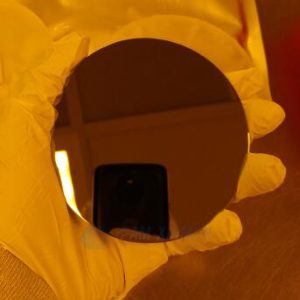
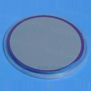
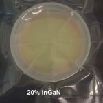
1. 2″ (50.8mm) Indium Gallium Nitride Epitaxy on Sapphire Template
| Item | GANW-INGAN-S |
| Conduction Type | Semi-insulating |
| Diameter | 50.8mm ± 1mm |
| Thickness: | 100-200nm, custom |
| Substrate: | sapphire |
| Orientation : | C-axis(0001)+/-1° |
| Dopant | In 5%~25% |
| XRD(102) | <400arc.sec |
| XRD(002) | <350arc.sec |
| Structure | InGaN/GaN buffer/Sapphire |
| Useable Surface Area | ≥90% |
| Surface Finish | Single or Double Side Polished,epi-ready |
2. Applications of InGaN Material
Indium gallium nitride (InGaN, InxGa1−xN) is a semiconductor material made of GaN and InN, which is used in LED as indium gallium nitride quantum wells, photovoltaics, quantum heterostructures or as InGaN on sapphire template. Specifically as follows:
LED: Indium gallium nitride is the light-emitting layer in modern blue and green LEDs and is usually grown on a GaN buffer layer on a transparent substrate (such as sapphire or silicon carbide). It has a high heat capacity and low sensitivity to ionizing radiation (like other Group III nitrides), which makes it a potentially suitable material for solar photovoltaic devices, especially satellite arrays.
Photovoltaic: The ability to use InGaN to perform band gap engineering within a range that provides a good spectral match with sunlight makes indium gallium nitride fabrication suitable for solar photovoltaic cells. It is possible to grow multiple layers with different band gaps because the material is relatively insensitive to defects introduced by the lattice mismatch between the layers. Two-layer multi-junction cells with band gaps of 1.1 eV and 1.7 eV can theoretically achieve a maximum efficiency of 50%. By depositing multiple layers adjusted to a wide range of band gaps, the theoretical efficiency is expected to reach 70%.
Quantum heterostructure: Quantum heterostructures are usually constructed from GaN with an indium gallium nitride active layer. InGaN can be combined with other materials, such as GaN, AlGaN, SiC, sapphire and even silicon.
Remark:
The Chinese government has announced new limits on the exportation of Gallium materials (such as GaAs, GaN, Ga2O3, GaP, InGaAs, and GaSb) and Germanium materials used to make semiconductor chips. From August 1, 2023 on, exporting these materials is only allowed if we obtains a license from the Chinese Ministry of Commerce. Hope for your understanding!