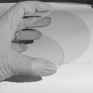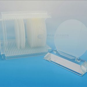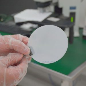
N Type Freestanding GaN Substrate

Ganwafer has established a series manufacturing technology for GaN substrates of various orientations, crystalline GaN Wafer and electrical conductivity and related III-N materials. More specifications of N-type GaN substrate please see below:
- Description
- Inquiry
Description
1. Specification of N Type GaN Freestanding Substrate
1.1 4″ N-Type -Doped GaN Free-standing Substrate
| Item | GANW-FS-GaN100-N+ |
| Conduction Type | N type/Si doped |
| Size | 4″(100)+/-1mm |
| Thickness | 480+/-50 |
| Orientation | C-axis(0001)+/-0.5° |
| Primary Flat Location | (10-10)+/-0.5° |
| Primary Flat Length | 32+/-1mm |
| Secondary Flat Location | (1-210)+/-3° |
| Secondary Flat Length | 16+/-1mm |
| Resistivity(300K) | <0.05Ω·cm |
| Dislocation Density | <5×10^6cm-2 |
| FWHM | <=100arc.sec |
| TTV | <=30um |
| BOW | <=+/-30um |
| Surface Finish | Front Surface:Ra<=0.3nm.Epi-ready polished |
| — | Back Surface: 1. Fine ground |
| — | 2. Polished |
| Usable Area | ≥ 90 % |
1.2 4″ Low Doped GaN, N Type
| Item | GANW-FS-GaN100-N- |
| Conduction Type | N type/low doped |
| Size | 4″(100)+/-1mm |
| Thickness | 480+/-50 |
| Orientation | C-axis(0001)+/-0.5° |
| Primary Flat Location | (10-10)+/-0.5° |
| Primary Flat Length | 32+/-1mm |
| Secondary Flat Location | (1-210)+/-3° |
| Secondary Flat Length | 16+/-1mm |
| Resistivity(300K) | <0.5Ω·cm |
| Dislocation Density | <5×10^6cm-2 |
| FWHM | <=100arc.sec |
| TTV | <=30um |
| BOW | <=+/-30um |
| Surface Finish | Front Surface:Ra<=0.3nm.Epi-ready polished |
| — | Back Surface: 1. Fine ground |
| — | 2. Polished |
| Usable Area | ≥ 90 % |
1.3 2″ Si-Doped GaN Film
| Item | GANW-FS-GaN50-N+ |
| Conduction Type | N type/Si doped |
| Size | 2″(50.8)+/-1mm |
| Thickness | 400+/-50 |
| Orientation | C-axis(0001)+/-0.5° |
| Primary Flat Location | (10-10)+/-0.5° |
| Primary Flat Length | 16+/-1mm |
| Secondary Flat Location | (1-210)+/-3° |
| Secondary Flat Length | 8+/-1mm |
| Resistivity(300K) | <0.05Ω·cm |
| Dislocation Density | <5×10^6cm-2 |
| FWHM | <=100arc.sec |
| TTV | <=15um |
| BOW | <=+/-20um |
| Surface Finish | Front Surface: Ra<=0.3nm. Epi-ready polished |
| — | Back Surface: 1. Fine ground |
| — | 2. Polished |
| Usable Area | ≥ 90 % |
1.4 2″ Low Doped N Type GaN Thin Film
| Item | GANW-FS-GaN50-N- |
| Conduction Type | N type/low doped |
| Size | 2″(50.8)+/-1mm |
| Thickness | 400+/-50 |
| Orientation | C-axis(0001)+/-0.5° |
| Primary Flat Location | (10-10)+/-0.5° |
| Primary Flat Length | 16+/-1mm |
| Secondary Flat Location | (1-210)+/-3° |
| Secondary Flat Length | 8+/-1mm |
| Resistivity(300K) | <0.5Ω·cm |
| Dislocation Density | <5×10^6cm-2 |
| FWHM | <=100arc.sec |
| TTV | <=15um |
| BOW | <=+/-20um |
| Surface Finish | Front Surface: Ra<=0.3nm. Epi-ready polished |
| — | Back Surface: 1. Fine ground |
| — | 2. Polished |
| Usable Area | ≥ 90 % |
2. Application of GaN Substrate
At present, the application of GaN is still dominated by the military, and it has gradually begun to move towards commercial fields, such as unmanned vehicles, wireless communication base stations, etc. And there are broad application prospects in white light LEDs, short-wavelength lasers, ultraviolet detectors, and high-temperature high-power devices. The largest application of GaN substrates (like semi-insulating / P type / N type GaN thin film) currently belongs to lasers, which are mainly used in the production of blue laser diodes. These products have been used as key components in Blu-ray Discs and HD-DVDs. In addition, these lasers fabricated on GaN substrate with ohmic contact are also very suitable for projection display, high-precision printing and optical sensing fields.
Moreover, there are potential GaN wafer market in optical detectors, which mainly include flame sensing, ozone monitoring, pollution monitoring, blood analysis, mercury lamp disinfection monitoring, laser detectors and other applications that require solar blind zone characteristics.
It is foreseeable that with the gradual maturity of GaN substrate technology, low-cost, high-quality GaN substrates are expected to be widely used in the fields of semiconductor microelectronic devices and optoelectronic devices.
Remark:
The Chinese government has announced new limits on the exportation of Gallium materials (such as GaAs, GaN, Ga2O3, GaP, InGaAs, and GaSb) and Germanium materials used to make semiconductor chips. From August 1, 2023 on, exporting these materials is only allowed if we obtains a license from the Chinese Ministry of Commerce. Hope for your understanding!