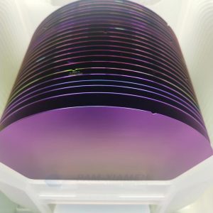
CZ Silicon Wafer


CZ silicon (Si) wafer produced by Ganwafer is grown by Czochralski (CZ) method, which is the mainstream technology for monocrystalline silicon growth with low cost established in the 1950s. In Czochralski method, the raw poly-silicon block is put into a quartz crucible, heated and melted in a single crystal furnace, and then a rod-shaped seed (seed crystal) with a diameter of only 10 mm is immersed in the melt. At a suitable temperature, the silicon atoms in the melt will be arranged along the silicon atoms of the seed and form regular crystals at the solid-liquid interface to become single crystals. Czochralski method can be used to manufacture 2 “, 4”, 8”, 12“ semiconductor polished wafers, epitaxial wafers, SOI and other semiconductor silicon wafers, mainly used in logic, memory chips and low-power integrated circuit components.
- Description
- Inquiry
Description
1. Specifications of CZ Silicon Wafer
1.1 12 inch CZ Silicon Wafer
| 12 inch CZ Silicon Wafer | |||
| Item | Parameters | ||
| Material | Monocrystalline Silicon | ||
| Grade | Prime Grade | ||
| Growth Method | CZ | ||
| Diameter | 300.0±0.3mm, 12″ | 300.0±0.3mm, 12″ | 300.0±0.3mm, 12″ |
| Conductivity type | Intrinsic | N Type | P Type |
| Dopant | low doped | Phosphorus | Boron |
| Orientation | [111]±0.5° | [100]±0.5° | (100)±0.5° |
| Thickness | 500±15μm | 500±25μm | 775±25μm |
| Resistivity | >10,000Ωcm | 0-10Ωcm | 1-10Ωcm |
| RRV | <40% (ASTM F81 Plan C) | ||
| SEMI STD Notch | SEMI STD Notch | SEMI STD Notch | SEMI STD Notch |
| Surface Finish | 1SP, SSP One-Side-Epi-Ready-Polished, Back Side Etched |
1SP, SSP One Side Polished Back Side Acid Etched |
1SP, SSP One Side Polished Back Side Acid Etched |
| Edge Rounded | Edge Rounded Per SEMI Standard | Edge Rounded Per SEMI Standard | Edge Rounded Per SEMI Standard |
| Particle | <20counts @0.3μm | ||
| Roughness | <1nm | ||
| TTV | <10um | <10um | <10um |
| Bow/Warp | <30um | <40um | <40um |
| TIR | <5µm | ||
| Oxygen Content | <2E16/cm3 | ||
| Carbon Content | <2E16/cm3 | ||
| OISF | <50/cm² | ||
| STIR (15x15mm) | <1.5µm | ||
| Surface Metal Contamination Fe,Zn, Cu,Ni, K,Cr |
≤5E10 atoms/cm2 | ||
| Dislocation Density | SEMI STD | SEMI STD | 500 max/ cm2 |
| Chips, scratches, bumps, haze, touch marks, orange peel, pits, cracks, dirt, contamination | All None | ||
| Laser Mark | SEMI STD | Option Laser Serialized: Shallow laser |
Along The Flat On The Front Side |
1.2 8 inch CZ Silicon Wafer with TTV<6μm
| 8 inch CZ Silicon Wafer with TTV<6μm | |||
| Item | Parameters | ||
| Material | Monocrystalline Silicon | ||
| Grade | Prime Grade | ||
| Growth Method | CZ | ||
| Diameter | 200.0±0.5mm, 8″ | 200.0±0.5mm, 8″ | 200.0±0.2mm, 8″ |
| Conductivity type | P Type | P Type | P Type |
| Dopant | Boron | Boron | Boron |
| Orientation | [111]±0.5° | [100]±0.5° | (111)±0.5° |
| Thickness | 1,000±15μm | 725±50μm | 1,000±25 μm |
| Resistivity | <1Ωcm | 10-40Ωcm | <100 Ωcm |
| RRV | <40% (ASTM F81 Plan C) | ||
| SEMI STD Notch | SEMI STD Notch | SEMI STD Notch | SEMI STD Notch |
| Surface Finish | 1SP, SSP One-Side-Epi-Ready-Polished, Back Side Etched |
1SP, SSP One Side Polished Back Side Acid Etched |
1SP, SSP One Side Polished Back Side Acid Etched |
| Edge Rounded | Edge Rounded Per SEMI Standard | Chamfer width 250-350μm | Edge Rounded Per SEMI Standard |
| Particle | <10counts @0.3μm | <20counts @0.3μm | <10counts @0.3μm |
| Roughness | <1nm | ||
| TTV | <6um | <10um | <6um |
| Bow/Warp | <60um | <40um | <60um |
| TIR | <5µm | ||
| Oxygen Content | <2E16/cm3 | ||
| Carbon Content | <2E16/cm3 | ||
| OISF | <50/cm² | ||
| STIR (15x15mm) | <1.5µm | ||
| Surface Metal Contamination Fe,Zn, Cu,Ni, K,Cr |
≤5E10 atoms/cm2 | ||
| Dislocation Density | SEMI STD | SEMI STD | < 10-2 cm-2 |
| Chips, scratches, bumps, haze, touch marks, orange peel, pits, cracks, dirt, contamination | All None | ||
| Laser Mark | SEMI STD | Option Laser Serialized: Shallow laser |
Along The Flat On The Front Side |
1.3 6 inch CZ Silicon Wafer with Particle<20counts @0.3μm
| 6 inch CZ Silicon Wafer with Particle<20counts @0.3μm | |||
| Item | Parameters | ||
| Material | Monocrystalline Silicon | ||
| Grade | Prime Grade | ||
| Growth Method | CZ | ||
| Diameter | 6″(150.0±0.5mm) | ||
| Conductivity type | P Type | P Type | P Type |
| Dopant | Boron | Boron | Boron |
| Orientation | <111>±0.5° | [111]±1° | (100)±0.5° |
| Thickness | 675±25μm | 675±10μm 1,000±25µm |
675±25μm |
| Resistivity | 0.1-13Ωcm | 0.01-0.02 Ωcm | 1-100Ωcm |
| RRV | <40% (ASTM F81 Plan C) | ||
| Primary Flat | SEMI STD | SEMI STD | SEMI STD |
| Secondary Flat | SEMI STD | SEMI STD | SEMI STD |
| Surface Finish | 1SP, SSP One Side Polished, Epi-ready Back Side Acid Etched |
1SP, SSP One Side Polished Back Side Acid Etched |
1SP, SSP One Side Polished Back Side Acid Etched |
| Edge Rounded | Edge Rounded Per SEMI Standard | Edge Rounded Per SEMI Standard | Edge Rounded Per SEMI Standard |
| Particle | <20counts @0.3μm | ≤10@≥0.3μm | |
| Roughness | <0.5nm | <1nm | <0.5nm |
| TTV | <10um | <10um | <12um |
| Bow/Warp | <30um | <40um | <60um |
| TIR | <5µm | ||
| Oxygen Content | <2E16/cm3 | ||
| Carbon Content | <2E16/cm3 | ||
| OISF | <50/cm² | ||
| STIR (15x15mm) | <1.5µm | ||
| Surface Metal Contamination Na, Al, K, Fe, Ni, Cu, Zn |
≤5E10 atoms/cm2 | ||
| Dislocation Density | SEMI STD | SEMI STD | 500 max/ cm2 |
| Chips, scratches, bumps, haze, touch marks, orange peel, pits, cracks, dirt, contamination | All None | All None | Tarnish, orange peel, contamination, haze, micro scratch, chips, edge chips, crack, crow feet, pin hole, pits, dent, waviness, smudge&scar on the back side: all none |
| Laser Mark | SEMI STD | SEMI STD | SEMI STD |
1.4 4 inch CZ Silicon Wafer
| 4 inch CZ Silicon Wafer | |||
| Item | Parameters | ||
| Material | Monocrystalline Silicon | ||
| Grade | Prime Grade | ||
| Growth Method | CZ | ||
| Diameter | 4″(100.0±0.5mm) | ||
| Conductivity type | P or N type | P Type | — |
| Dopant | Boron or Phosphorus | Boron | — |
| Orientation | <100>±0.5° | — | (100) or (111)±0.5° |
| Thickness | 525±25μm | 525±25μm | 300±25μm |
| Resistivity | 1-20Ωcm | 0.002 – 0.003Ωcm | 5-10Ohmcm |
| RRV | <40% (ASTM F81 Plan C) | ||
| Primary Flat | SEMI STD Flats | SEMI STD Flats | 32.5+/-2.5mm, @110±1° |
| Secondary Flat | SEMI STD Flats | SEMI STD Flats | 18±2mm, @90°±5° to Primary Flat |
| Surface Finish | One-Side-Epi-Ready-Polished, Back Side Etched |
||
| Edge Rounded | Edge Rounded Per SEMI Standard | ||
| Particle | <20counts @0.3μm | ||
| Roughness | <0.5nm | ||
| TTV | <10um | ||
| Bow/Warp | <40um | ||
| TIR | <5µm | ||
| Oxygen Content | <2E16/cm3 | ||
| Carbon Content | <2E16/cm3 | ||
| OISF | <50/cm² | ||
| STIR (15x15mm) | <1.5µm | ||
| Surface Metal Contamination Fe,Zn, Cu,Ni, K,Cr |
≤5E10 atoms/cm2 | ||
| Dislocation Density | 500 max/ cm2 | ||
| Chips, scratches, bumps, haze, touch marks, orange peel, pits, cracks, dirt, contamination | All None | ||
| Laser Mark | Along The Flat On The Front Side,option Laser Serialized: Shallow laser |
||
1.5 2 inch CZ Si Wafer
| 2 inch CZ Silicon Wafer | |||
| Item | Parameters | ||
| Material | Monocrystalline Silicon | ||
| Grade | Prime Grade | ||
| Growth Method | CZ | ||
| Diameter | 2″(50.8±0.5mm) | ||
| Conductivity type | P or N type | — | P Type |
| Dopant | Boron or Phosphorus | — | Boron |
| Orientation | <100> | (100) or (111)± 0.5° | — |
| Thickness | 150±25μm | 275±25μm | — |
| Resistivity | 1-200Ωcm | — | 0.01-0.02Ωcm |
| RRV | <40% (ASTM F81 Plan C) | ||
| Primary Flat | SEMI STD Flats | ||
| Secondary Flat | SEMI STD Flats | ||
| Surface Finish | One Side Polished Back Side Acid Etched |
||
| Particle | <20counts @0.3μm | ||
| Roughness | <0.5nm | <0.5nm | — |
| TTV | <10um | — | <10um |
| Bow/Warp | <30um | <20um | — |
| TIR | <5µm | ||
| Oxygen Content | <2E16/cm3 | ||
| Carbon Content | <2E16/cm3 | ||
| OISF | <50/cm² | ||
| STIR (15x15mm) | <1.5µm | ||
| Surface Metal Contamination Fe,Zn, Cu,Ni, K,Cr |
≤5E10 atoms/cm² | ||
| Dislocations | None | ||
| Chips, scratches, bumps, haze, touch marks, orange peel, pits, cracks, dirt, contamination | All None | ||
2. Nitrogen in Czochralski Process of Silicon Wafers
Nitrogen plays a very important role in CZ silicon ingots, and a small amount of nitrogen doping will have a beneficial effect on the performance of single crystal silicon. There are many methods for actively adding nitrogen: Using nitrogen protection during the CZ silicon crystal growing process or adding silicon nitride powder to the molten silicon; and nitrogen ion implantation. At a temperature of about 1415 degrees, the saturated solubility of nitrogen in silicon melt and single crystal silicon is 6×1018cm-3 and 4.5×1015cm-3, respectively. Since the equilibrium segregation coefficient of nitrogen in silicon is 7×10⁻⁴, the concentration of nitrogen during the growth of silicone CZ is generally less than 5×1015 cm-3.
The interaction of nitrogen and oxygen in Czochralski single crystal silicon can form a nitrogen-oxygen complex, which exhibits multiple absorption peaks in the mid-infrared and far-infrared absorption spectra. The nitrogen-oxygen complex is a kind of shallow donor and has electrical activity. Combining infrared absorption and resistivity tests, it can be found that with the disappearance of the infrared absorption peak of the nitrogen-oxygen complex during the annealing process, the resistivity or carrier concentration of the single crystal silicon wafer semiconductor will change accordingly. The electrical activity of the nitrogen-oxygen complex can be eliminated by high-temperature annealing. Doping nitrogen in CZ single crystal Si wafer has an inhibitory effect on the formation of thermal donors and new donors.
Doping nitrogen into large-size Czochralski silicon can change the size and density of void-type defects, so that the void-type defects can be easily eliminated by high-temperature annealing. In addition, the nitrogen can enhance the warpage resistance of CZ Si substrate and improve the yield of integrated circuits fabricated on Czochralski process silicon wafer.