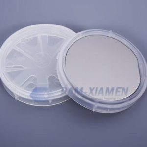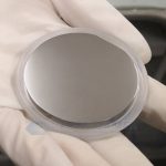
GaAs Wafer
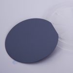
Single crystal Gallium Arsenide (GaAs) wafer is offered from Ganwafer – a leading GaAs substrate supplier for opto-electronics and micro-electronics industry for making LD, LED, microwave circuit and solar cell applications. The gallium arsenide substrates are in diameter range from 2″ to 6″ in various thicknesses and orientations. We offer single crystal GaAs substrates produced by VGF method, allowing us to provide customers the widest choice of GaAs material with high uniformity of electrical properties and excellent surface quality.
- Description
- Inquiry
Description
1. Specifications of GaAs Wafer
1.1 Gallium Arsenide (GaAs) Wafer for LED Applications
| Item | Specifications | Remarks |
| Conduction Type | SC/n-type | SC/p-type with Zn dope Available |
| Growth Method | VGF | |
| Dopant | Silicon | Zn available |
| Wafer Diameter | 2, 3 & 4 inch | Ingot or as-cut available |
| Crystal Orientation | (100)2°/6°/15° off (110) | Other misorientation available |
| OF | EJ or US | |
| Carrier Concentration | (0.4~2.5)E18/cm3 | |
| Resistivity at RT | (1.5~9)E-3 Ohm.cm | |
| Mobility | 1500~3000cm2/V.sec | |
| Etch Pit Density | <5000/cm2 | |
| Laser Marking | upon request | |
| Surface Finish | P/E or P/P | |
| Thickness | 220~450um | |
| Epitaxy Ready | Yes | |
| Package | Single wafer container or cassette | |
1.2 Single Crystal Gallium Arsenide Substrate for LD Applications
| Item | Specifications | Remarks |
| Conduction Type | SC/n-type | |
| Growth Method | VGF | |
| Dopant | Silicon | |
| Wafer Diameter | 2, 3 & 4 inch | Ingot or as-cut available |
| Crystal Orientation | (100)2°/6°/15°off (110) | Other misorientation available |
| OF | EJ or US | |
| Carrier Concentration | (0.4~2.5)E18/cm3 | |
| Resistivity at RT | (1.5~9)E-3 Ohm.cm | |
| Mobility | 1500~3000 cm2/V.sec | |
| Etch Pit Density | <500/cm2 | |
| Laser Marking | upon request | |
| Surface Finish | P/E or P/P | |
| Thickness | 220~350um | |
| Epitaxy Ready | Yes | |
| Package | Single wafer container or cassette | |
1.3 Semi-insulating Gallium Arsenide Wafer for Microelectronics Applications
| Item | Specifications | Remarks |
| Conduction Type | Insulating | |
| Growth Method | VGF | |
| Dopant | C doped | |
| Wafer Diameter | 2, 3 & 4 inch | Ingot available |
| Crystal Orientation | (100)+/- 0.5° | |
| OF | EJ, US or notch | |
| Carrier Concentration | n/a | |
| Resistivity at RT | >1E7 Ohm.cm | |
| Mobility | >5000 cm2/V.sec | |
| Etch Pit Density | <8000 /cm2 | |
| Laser Marking | upon request | |
| Surface Finish | P/P | |
| Thickness | 350~675um | |
| Epitaxy Ready | Yes | |
| Package | Single wafer container or cassette | |
1.4 150mm GaAs Wafer Substrate, Semi-insulated for Microelectronics Applications (including Fabrication of THz Photoconductive Antennas)
| Item | Specifications | Remarks |
| Conduction Type | Semi-insulating | – |
| Grow Method | VGF | – |
| Dopant | C doped | – |
| Type | N | – |
| Diameter(mm) | 150±0.25 | – |
| Orientation | (100)0°±3.0° | – |
| NOTCH Orientation | (010)±2° | – |
| NOTCH Depth(mm) | (1-1.25)mm 89°-95° | – |
| Carrier Concentration | please consult our sales team | – |
| Resistivity(ohm.cm) | >1.0×10⁷ or 0.8-9 x10⁻³ | – |
| Mobility(cm2/v.s) | please consult our sales team | – |
| Dislocation | please consult our sales team | – |
| Thickness(µm) | 675±25 | – |
| Edge Exclusion for Bow and Warp(mm) | please consult our sales team | – |
| Bow(µm) | please consult our sales team | – |
| Warp(µm) | ≤20.0 | – |
| TTV(µm) | ≤10.0 | – |
| TIR(µm) | ≤10.0 | – |
| LFPD(µm) | please consult our sales team | – |
| Polishing | P/P Epi-Ready | – |
1.5 2″ LT-GaAs (Low Temperature-Grown Gallium Arsenide) Wafer Specifications
| Item | Specifications |
| Conduction Type | Semi-insulating |
| Grow Method | VGF |
| Dopant | C doped |
| Type | N |
| Diameter(mm) | 150±0.25 |
| Orientation | (100)0°±3.0° |
| NOTCH Orientation | (010)±2° |
| NOTCH Depth(mm) | (1-1.25)mm 89°-95° |
| Carrier Concentration | please consult our sales team |
| Resistivity(ohm.cm) | >1.0×10⁷ or 0.8-9 x10⁻³ |
| Mobility(cm2/v.s) | please consult our sales team |
| Dislocation | please consult our sales team |
| Thickness(µm) | 675±25 |
| Edge Exclusion for Bow and Warp(mm) | please consult our sales team |
| Bow(µm) | please consult our sales team |
| Warp(µm) | ≤20.0 |
| TTV(µm) | ≤10.0 |
| TIR(µm) | ≤10.0 |
| LFPD(µm) | please consult our sales team |
| Polishing | P/P Epi-Ready |
Gallium arsenide substrate can be used as a substrate material for epitaxial growth of other semiconductors such as aluminum gallium arsenide (AlGaAs) and indium gallium arsenide (InGaAs). Direct gallium arsenide band gap can effectively emit and absorb light. Gallium arsenide single crystal wafer has extremely high electron mobility, which allows GaAs transistors to work at frequencies exceeding 250 GHz and reduces noise. High frequencies tend to reduce electrical signal interference in electronic circuits.
2. Q&A of Gallium Arsenide Wafer
2.1 What is the GaAs Process?
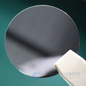
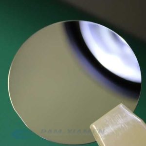
Before device fabrication, GaAs wafers must be completely cleaned to remove any damage occurred during the dicing process. After cleaning, the gallium arsenide wafers are chemically mechanically polished/plaranrized (CMP) for the final material removal stage. This CMP process allows for the attainment of super-flat mirror-like surfaces with a remaining roughness on an atomic scale. And then, the gallium arsenide semiconductor wafer is ready for fabrication.
2.2 What is GaAs Wafer?
Gallium arsenide (GaAs) is a compound of gallium and arsenic, which is a III-V direct band gap semiconductor with a zinc blende crystal structure.
Gallium arsenide wafer is an important semiconductor material. It belongs to group III-V compound semiconductor. It is a sphalerite type lattice structure with a lattice constant of 5.65×10⁻¹⁰m, a melting point of 1237℃ and a band gap of 1.4 EV. GaAs single crystal can be made into semi insulating high resistance materials with resistivity higher than silicon and germanium by more than three orders of magnitude, which can be used to make integrated circuit substrate, infrared detector, γ photon detector, etc. Because the electron mobility of gallium arsenide substrate is 5-6 times larger than that of silicon, gallium arsenide wafer for sale has been widely used in microwave devices and high-speed digital circuits. The semiconductor device made of GaAs has the advantages of high frequency, high temperature and low temperature, low noise and strong radiation resistance. Due to the excellent gallium arsenide properties, it can also be used to make bulk effect devices.
Remark:
The Chinese government has announced new limits on the exportation of Gallium materials (such as GaAs, GaN, Ga2O3, GaP, InGaAs, and GaSb) and Germanium materials used to make semiconductor chips. From August 1, 2023 on, exporting these materials is only allowed if we obtains a license from the Chinese Ministry of Commerce. Hope for your understanding!