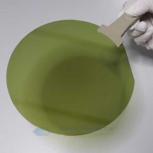
SiC Epi Wafer
SiC epitaxial wafer is a kind of silicon carbide wafer that a single crystal film (epitaxial layer) with certain requirements and the same crystal as the substrate is grown on the SiC substrate. In practical applications, almost all wide bandgap semiconductor devices are fabricated on epitaxial wafers, while silicon carbide wafer itself is only used as substrate, including the substrate for GaN epitaxial growth.
- Description
- Inquiry
Description
Compared with traditional Si-based power devices, SiC single crystal materials cannot directly fabricate the SiC power device. SiC epitaxy wafer with high quality must be grown on SiC conductive substrate. Then, use the SiC epi wafers to fabricate the devices.
Epitaxial is an important process in the whole semiconductor industry flow. Because devices are almost obtained by epitaxial growth, the quality of silicon carbide epitaxial wafer will make a great effect on the devices’ performance. In addition, the epitaxial is in the middle position of the whole semiconductor process, which is greatly affected by crystal and substrate processing. All in all, epitaxial process plays an important part in the development of the industry.
1. Specification of SiC Epitaxial Wafer
1.1 Specification of 4” Silicon Carbide Epitaxial Wafer
| Items | N-type | Typical | P-type | Typical |
| Specification | Specification | |||
| Diameter | 4″(100 mm) | — | 4″(100 mm) | — |
| Poly-type | 4H | — | 4H | — |
| Surface | (0001) Silicon-face | — | (0001) Silicon-face | — |
| Off-orientation toward <11-20> | 4 deg-off | — | 4 deg-off | — |
| Conductivity | n-type | — | p-type | — |
| Dopant | Undoped, Nitrogen | — | Aluminum | — |
| Carrier Concentration | <1E14,2E14-2E19 cm-3 | — | 2E14-2E19 cm-3 | — |
| Tolerance | ±18% | ±14% | ±48% | ±24% |
| Uniformity | < 14% | 8% | < 19% | 14% |
| Thickness Range | 0.5-100 μm | — | 0.5-30 μm | — |
| Tolerance | 8% | ±4% | ±8% | ±4% |
| Uniformity | < 5% | 1.80% | < 5% | 1.80% |
1.2 Specification of 6” SiC Epi Wafer
| Items | N-type | Typical | P-type | Typical |
| Specification | Specification | |||
| Diameter | 6″(150 mm) | — | 6″(150 mm) | — |
| Poly-type | 4H | — | 4H | — |
| Surface | (0001) Silicon-face | — | (0001) Silicon-face | — |
| Off-orientation toward <11-20> | 4 deg-off | — | 4 deg-off | — |
| Conductivity | n-type | — | p-type | — |
| Dopant | Undoped, Nitrogen | — | Aluminum | — |
| Carrier Concentration | <1E14,2E14-2E19 cm-3 | — | 2E14-2E19 cm-3 | — |
| Tolerance | ±18% | ±14% | ±48% | ±24% |
| Uniformity | < 14% | 0.08 | < 19% | 0.14 |
| Thickness Range | 0.5-80 μm | — | 0.5-30 μm | — |
| Tolerance | 0.08 | ±4% | ±8% | ±4% |
| Uniformity | < 5% | 2% | < 5% | 2% |
Note:
* In SiC epi wafer market, all the SiC substrate for epi growth is production grade, and the edge exclusion should be 3mm;
* N-type epi layers <20 microns are preceded by n-type, E18 cm-3, 0.5 μm buffer layer;
* N-type epi layers≥20 microns are preceded by n-type, E18, 1-5 μm buffer layer;
* Not all doping densities are available in all thickness;
* N-type doping is determined as an average value across the wafer (17 points) using Hg probe CV;
* SiC wafer thickness is determined as an average value across the wafer (9 points) using FTIR;
* Uniformity: standard deviation (σ)/average.
2. What is the Difference Between SiC Epitaxy and Silicon Epitaxy?
The SiC substrate is usually grown by PVT with the temperature as high as 2000℃. However, the production cycle is long; the output is low. Compared with silicon substrate, the cost of SiC substrate is very high.
As for the epitaxial process, SiC epitaxy process is almost same with silicon’s, but there will be a bit differences in temperature design and structure design.
Due to the particularity of materials, the device processing technology is different from silicon. High temperature processes including ion implantation, oxidation and annealing are adopted.
3. What is the Key Parameters of Silicon Carbide Epi Wafer?
Thickness and doping concentration uniformity are the most basic and key parameters of SiC epitaxial materials. Actually, the parameters of SiC epi wafer are depended on the device design. Take the following case as an example: different voltage levels of the devices will determine the epitaxial parameters. Specifically, the SiC wafer epitaxial thickness should be 6um at a low voltage of 600V; the SiC wafer thickness should be 10~15um at a medium voltage of 1200~1700V; the thickness of silicon carbide epitaxial layers should be more than 100um at a voltage >= 10000. The epitaxial thickness increases along with the voltage capability increases. It is more difficult to grow high quality SiC epi wafers since there is a great challenge in defect control, especially in high voltage application.
In fact, SiC epi has many defects. Due to different crystals, their defects are also different. The defects mainly include microtubules, triangular defects, surface carrot defects, ladder aggregation and other special defects. It is worth noting that many defects are directly from the substrate. Therefore, the quality and processing level of the substrate, particularly the control of defects, are very important for epitaxial growth.
SiC epitaxial defects are generally classified into fatal and non-fatal one. Fatal defects, such as triangle defects and droppings, have an impact on all types of devices, including diodes, MOSFETs and bipolar devices. The biggest impact is the breakdown voltage, which can reduce the breakdown voltage by 20% or even 90%. Non-fatal defects, such as some TSD and TED, may have no effect on the diode, and may have an impact on the life of MOS and bipolar devices, or have some effect of leakage, which will eventually affect the processing qualification rate of the device.
Silicon carbide epitaxial defects are generally divided into fatal defects and non-fatal defects. Fatal defects such as triangular defects and dripping can affect all types of devices, like diodes, MOSFETs and bipolar devices. The biggest influence is the breakdown voltage, dropped from 20%, even 90%. Non-fatal defects, like some TSDs and Ted, may not affect the diodes, but may affect the service life of MOS and bipolar devices, or have a certain leakage effect. Eventually, it will affect the device processing qualification rate.
Following are several suggestions for controlling epitaxial defects of SiC wafer production:
Firstly, select the substrate material carefully;
Secondly, select the equipment and localization;
Thirdly, choose proper process technology.
4. What Progress of SiC Epitaxial Technology?
In the medium and low voltage field, the thickness and doping concentration of SiC epitaxial wafer can be relatively good. However, in the high voltage field, there are still many difficulties, including thickness, uniformity of doping concentration, triangular defects and so on, to be overcome.
In the medium and low voltage applications, SiC epitaxy process is mature. SiC epitaxial thin film can meet the demands of SBD, JBS, MOS and other devices at medium and low voltage on the whole. The thickness and doping concentration of 10um epitaxial layers in 1200V device applications are obtained with a good level. The surface defects can reach less than 0.5 square meters.
In high voltage field, the silicon carbide epitaxy technology is relatively backward. A 200um SiC epitaxial wafer has a lot of uniformity, thickness and concentration for fabricating a 20000 V device. Meanwhile, the thick SiC film required by high voltage devices has many defects, especially the triangular defects. It will affect the high current devices’ preparation. A large chip area can produce a large current, and the lifetime of minority carrier will be low.
Regarding high voltage field, device types tend to use bipolar devices, requiring higher minority carrier lifetime. The minority carrier lifetime must be at least 5us or longer to obtain the ideal forward current. The minority carrier lifetime parameters of SiC epitaxial wafers are 1~2us. Thus, this is not so important for high-voltage devices now, but needs subsequent technical treatment.
5. What is the Fabrication Technology of SiC Epi Wafer?
Silicon carbide epitaxy has two major technologies in equipment:
1/Step flow growth model proposed in 1980: This plays a very important role in the development and quality of epitaxy. It can be grown at relatively low temperature. At the same time, it can achieve very stable control for the 4H crystal form which we are interested in TCS is introduced to improve the growth rate.
2/The introduction of TCS can achieve the growth rate more than 10 times of the traditional growth rate. The introduction of TCS not only improves the production rate, but also greatly controls the quality, especially for the control of silicon droplets. Therefore, it is very beneficial for thick film epitaxial growth. This technology was first commercialized by LPE in 14 years. In about 17 years, Aixtron upgraded the equipment and transplanted the technology to commercial equipment.