")
AlGaN on Sapphire/Silicon
AlGaN (aluminum gallium nitride) template is a semiconductor wafer, which is composite of aluminum nitride and gallium nitride, and the AlxGa1−xN band gap can be tailored from 3.4eV (xAl=0) to 6.2eV (xAl=1). Al% of AlGaN composition can be 0.1-0.5. Compared with GaN, AlGaN has a wider band gap and higher dielectric breakdown strength, and it is expected to produce power devices with lower losses than GaN.
The application of AlGaN semiconductor is for LED, LD, and HEMT structure. And now please see below specification:
- Description
- Inquiry
Description
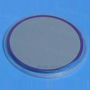
Ganwafer offers AlGaN template, which AlGaN layers are commonly grown on sapphire or (111) Si substrate. Our AlGaN epitaxial wafer fab can also make aluminum gallium nitride semiconductor wafer with additional GaN layers. Sapphire is one of the most commonly material used for growing AlGaN template. Due to the large lattice mismatch and thermal mismatch between AlGaN-based material and sapphire substrate, AlGaN-based materials are usually grown on AIN/sapphire templates.
1. Specifications of AlGaN Template
1.1 2″ (50.8mm) AlGaN Epi on Sapphire Template
| Item | GANW-AlGaNT-SA-50 |
| Diameter | 50.8mm ± 0.4mm |
| Orientation : | C(0001), on axis |
| Conduction Type | – |
| Epi Layer Thickness: | 200nm-1000nm |
| Epi Layer Material | AlGaN(ex.Al(0.1)Ga(0.9)N) |
| Structure | AlGaN/AlN buffer/Sapphire Substrate |
| Substrate: | sapphire |
| Orientation Flat | A-plane |
| XRD FWHM of (0002) | <200 arcsec. |
| Useable Surface Area | ≥90% |
| Surface: | Single side polished, Epi-ready |
1.2 4″ (100mm) Aluminum Gallium Nitride Films on Sapphire Template
| Item | GANW-AlGaNT-SA-100 |
| Diameter | 100mm ± 0.4mm |
| Orientation : | C(0001), on axis |
| Conduction Type | – |
| Epi Layer Thickness: | 2um,3um |
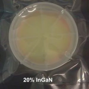
| Epi Layer Material | AlGaN(ex.Al(0.2)Ga(0.8)N) |
| Structure | AlGaN/AlN buffer/Sapphire Substrate |
| Substrate: | sapphire |
| Orientation Flat | A-plane |
| XRD FWHM of (0002) | <200 arcsec. |
| Useable Surface Area | ≥90% |
| Surface: | Single side polished, Epi-ready |
1.3 6″ (150mm) AlGaN Semiconductor Template on Silicon
| Item | GANW-AlGaNT-Silicon-150 |
| Diameter | 150mm ± 0.4mm |
| Orientation : | C(0001), on axis |
| Conduction Type | – |
| Epi Layer Thickness: | 200nm-3000nm |
| Epi Layer Material | AlGaN(ex.Al(0.2)Ga(0.8)N) |
| Structure | AlGaN/AlN buffer/Sapphire Substrate |
| Substrate: | 6”,Silicon, p type, (111), 1000um thick |
| Orientation Flat | – |
| XRD FWHM of (0002) | -arcsec. |
| Useable Surface Area | ≥90% |
| Surface: | Single side polished, Epi-ready |
2. About AlGaN Semiconductor Material
As an important third-generation direct band gap semiconductor material, Al-Ga-N ternary alloy has potential applications in the fields of ultraviolet guidance, ultraviolet warning and external communications. Since there is no natural AlGaN alloy, metal organic compound vapor deposition (MOCVD) or molecular beam epitaxy (MBE) is usually used to grow up to 2~3um AlGaN semiconductor materials on the sapphire wafer. In the aluminum gallium nitride, the content of aluminum is closely related to the material forbidden band width, which directly determines its application range. Therefore, it is of great significance to accurately determine the content of Al in AlGaN. At present, the determination of Al content in the AlGaN epitaxial layer usually adopts non-destructive physical methods, such as Rutherf backscattering method (RBS), ultraviolet visible light transmission method (UV-VIS), high resolution X-ray diffraction method (HRXRD) and electron Probe Micro Area Analysis (EPMA) and so on.
3. AlGaN Semiconductor Optical Properties
The AlGaN thin film is grown on a double-polished c-plane sapphire substrate using MOCVD technology. In order to further study the quality and linear optical properties of the optical film, the basic optical characterization of the film was carried out. At room temperature, the visible-ultraviolet spectrometer is used to measure that the Al-rich AlGaN semiconductor material has a sharp absorption boundary in the near ultraviolet region, and the position of the absorption boundary changes significantly with the Al content. It also shows that the incorporation of Al effectively modulates the gallium nitride material optical band gap.
Remark:
The Chinese government has announced new limits on the exportation of Gallium materials (such as GaAs, GaN, Ga2O3, GaP, InGaAs, and GaSb) and Germanium materials used to make semiconductor chips. From August 1, 2023 on, exporting these materials is only allowed if we obtains a license from the Chinese Ministry of Commerce. Hope for your understanding!