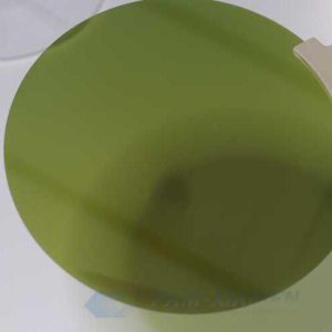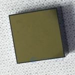
CdZnTe Wafer
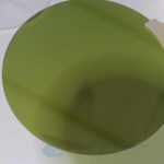
Cadmium zinc telluride (short for CdZnTe or CZT) wafer is an important II-VI group semiconductor material, which can be offered by CdZnTe wafer manufacturer – Ganwafer mainly for infrared thin film epitaxial growth and radiation detection. The band gap of CdZnTe is large, and low-energy infrared light cannot excite the electron conduction band transition in the valence band, so it does not produce intrinsic absorption of infrared light. Moreover, the dielectric constant of cadmium zinc telluride ingot is small, and the extinction coefficient is small when infrared is transmitted, so the infrared transmittance of CZT wafer is high. More important, the CZT lattice constant can be adjusted with different Zn content to meet the growth requirements of HgCdTe (MCT) epitaxial films with different compositions. More info about CdZnTe wafer please see below:
- Description
- Inquiry
Description
1. Cadmium Zinc Telluride (CZT) Wafer Specifications
1.1 CdZnTe for HgCdTe Epitaxial Growth
| CdZnTe For epitaxial growth, HgCdTe: | |
| CZT substrate size | 20×20 +/-0.1mm or larger |
| CZT structure | undoped twin-free |
| CZT thickness | 1000 +/- 50 |
| Zinc Distribution | 4.5% or custom |
| “y” % wafer to wafer | <4% +/- 1% |
| “y” % within wafer | <4% +/- 0.5% |
| Orientation | (211)B,(111)B |
| DCRC FWHM | <= 50 arc.sec |
| Carrier concentration | – |
| IR transmission % (2-20)um | >60% |
| Precipitate size | <5um |
| Precipitate density | <1E4 cm-2 |
| Etch pit density | <=1E5 cm-2 |
| Surface, B-face | EPI ready |
| Surface, A-face | Roughly polished |
| Surface roughness | Ra<20A or custom |
| Te precipitate size | <5um |
| Face identification | A face |
When the composition of Zn is 0.04, Cd0.96Zn0.04Te wafer is perfect for epitaxial HgCdTe film because its lattice constant and chemical properties are matched with the HgCdTe – an infrared detector material.
1.2 CdZnTe Wafer for Radiation Detection
The CdZnTe substrate with the composition Zn=0.1~0.2 can be provided with or without contacts. CZT substrate is the emerging nuclear radiation detector material in recent years. There are many excellent cadmium zinc telluride properties for this application: large band gap, easy to control heat current generation; large average atomic number, strong ability to stop rays, good mechanical strength, convenient for the production of devices; high resistivity, the manufactured detector can still maintain low leakage current under high bias voltage. Therefore, the detector noise is reduced. Compared with the traditional sodium iodide scintillator nuclear radiation detector, it has a higher energy resolution.
In addition, X-ray and Y-ray detectors made of zinc cadmium telluride crystal can work at room temperature, eliminating the trouble of adding liquid nitrogen. Moreover, the cadmium zinc telluride x-ray detector can be easily processed into a pixel array detector, and with the bridged silicon integrated signal readout circuit, it can be made into a compact, efficient, and high-resolution radiographic imaging device, which can be widely used in X-ray fluorescence analysis, nuclear waste monitoring, airport and port safety testing, industrial flaw detection, medical diagnosis, astrophysics research, etc.
1.3 Cadmium Zinc Telluride Substrate for Infrared and Photoelectric Devices
By adding a proper amount of vanadium (V) or indium (In) to cadmium zinc telluride, cadmium zinc telluride becomes an excellent near-infrared semiconductor photorefractive material. The strong demand for optical information processing in the near-infrared band has pushed the development of new types of near-infrared photorefractive materials. Doped with a proper amount of vanadium or indium during the CdZnTe growth, vanadium or indium becomes the photorefractive sensitive deep energy level center, so that the CdZnTe wafer material has a large photoelectric coefficient in the near-infrared band, which can be used to make near-infrared wave band real-time optical holographic memory and optical phase sharing device.
Because cadmium zinc telluride has a high infrared transmittance (~65%) in the infrared band, cadmium zinc telluride wafers can be used to make infrared lenses, prisms and other infrared optical components. Besides, the excellent photoelectric performance of CdZnTe crystal makes it suitable for the development of optoelectronic devices such as photoelectric modulators and thin-film solar cells.
2. Application of CdZnTe Wafer
In short, CdZnTe wafer can be used for:
* growth of high-quality HgCdTe epitaxial films;
* infrared laser window materials with excellent performance;
* production of X-ray and γ-ray detectors;
* production of quantum superlattice CdTe/ZnTe epitaxial wafer;
* solar cells;
* photoelectric modulators, etc.