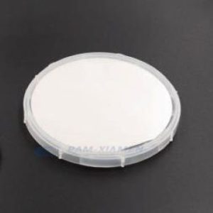
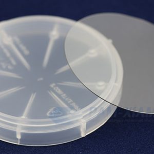
GaN epi on sapphire or silicon template is available with N-type, P-type, and semi-insulating type. Our gallium nitride (GaN) template is available in diameters from 2” up to 6”, and consists of a thin layer of crystalline GaN grown on a sapphire/silicon substrate. GaN films on sapphire and silicon from Ganwafer have extremely high breakdown voltage and industry-leading low defect control, which is used in power and electronic devices. Moreover, GaN on silicon wafer will be perfect for the outbreak of the 5G market and lead the future trend of the RF industry.
In earlier studies for GaN on sapphire substrate, evidence of microcrack formation in the sapphire substrate during GaN growth was found. But the formation of macrocracks extending to the GaN surface was thought to originate only from thermal mismatch. Later, when the GaN layers on sapphire grew beyond 100 mm, it was found that there was an efficient relaxation process for GaN template on sapphire. The growth of crack-free GaN-on-sapphire template approaching 2 inches in diameter has been demonstrated. It has been found that cracks are usually already formed during growth of GaN/sapphire template due to tensile strain formed during early nucleation. This early crack formation on GaN on sapphire template may have adverse effects; microcracks in the sapphire substrate may act as subsequent initial fracture points for relieving the increased strain due to the different coefficients of thermal expansion of the layers and the substrate during cooling. Even if growth conditions can be found that lead to crack healing during growth that holds true. The diffusivity of the grown GaN films on sapphire surface is considered an important parameter for the healing of such cracks.