Who Are Ganwafer?
Ganwafer is a top-class enterprise for compound semiconductor material integrating semiconductor crystal growth, process development, and epitaxy. We specialize in the research and production of compound semiconductor wafers such as SiC&GaN material (SiC wafer and epitaxy, GaN wafer and epi wafer) and III-V material (III-V substrate and epi service: InP wafer, GaSb wafer, GaAs wafer, InAs wafer, and InSb wafer).
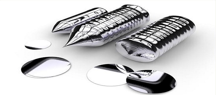
As a leading research and manufacturing company, we are dedicated to research and create CZ silicon wafer and ingot from 1990 and develop FZ silicon wafer with >1000 ohm.cm. We can able to deliver wafer sizes from 2” to 12” with prime grade and test grade.
Semiconductor wafers from Ganwafer are used in various applications. They are hugely used in LED semiconductor lighting, wireless communication, solar power, infrared device, laser, detectors, and semiconductor power devices, including power devices, high-temperature devices, and photoelectric devices, therein, GaN wafer including GaN on Si, GaN on SiC, and GaN on Sapphire are for Mini/micro LED, power electronics and microwave RF.
Why Ganwafer?
Our Strength
We have an expert team of a strong technical R & D team, leading by famous chief scientists, and have a strong R & D strength. We have the top wafer foundry to produce expected products effectively. Our experts have a great understanding of the latest material and devices as per the market trend that helps to develop new product types. We aim at constantly improving the quality of existing product.
Quality Product
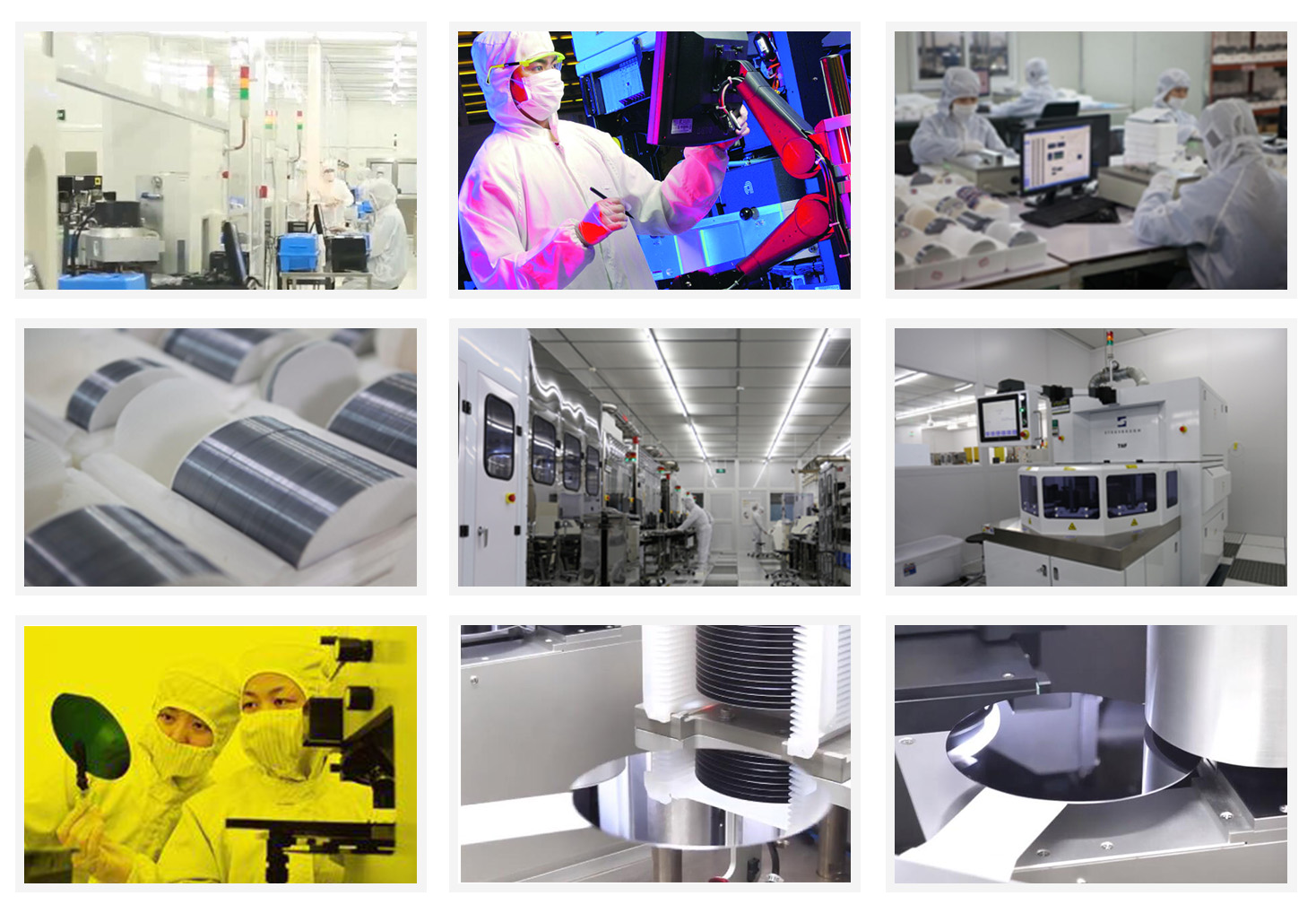
Ganwafer has been ISO9001:2015, owns and shares four modern foundries that able to deliver a range of industry-standard products with utmost quality. We ensure that our produced advanced wafer will meet clients’ needs, specifications, and budgets. We have been operating in this industry for many years that makes us stand out from the market. Each process of wafer manufacturing will be handled through our severe quality system. You can expect test reports for each shipment and each wafer are warranty.
25+ Years Experiences
We have a wealth of experience in material preparation and related equipment design and development as well as painstaking research on the physical, chemical, and electrical properties of materials, material preparation procedure. The vast knowledge of theoretical deposition and practical experience of scientific and technological personnel is the core power of our company.
The years of expertise in the expansion of pertinent materials and equipment guarantees better product quality & performance. Our equipment design scheme can meet the actual technical and technological requirements of users. Our rich history of materials development makes our company stand out from the market and set a benchmark in this industry as an industry-leading authority on a diverse range of compound semiconductor types.
Superior Quality
Providing top-quality products as per the industry standard without compromising the quality is our top priority. We ensure superior customer service. Our sales representatives will clear your queries and distributors ensure smooth customs and shipping procedures. Our esteemed customers can easily buy their products without any hassle. Customers will receive an affordable deal within their budget range and will get the best value for their money.
Good Sales Service
We understand that the requirements and specifications will vary with different clients and also the project size will vary. Do not bother at all! We are here to help you. We are capable enough to meet all of your requirements. Customers are free to ask their queries whatever they want to consult with our expert sales team. We ensure sustained and profitable growth for every customer, industry-standard products, and superior customer service.
Our History
Commercial CdZnTe (CZT) wafer are on mass production,which is a new semiconductor, which enables to convert radiation to electron effectively, it is mainly used in infrared thin-film epitaxy substrate, X-ray and γ-ray detection, laser optical modulation, high-performance solar cells and other high-tech fields.
Ganwafer has established the manufacturing technology for GaN epitaxy on Sapphire and freestanding GaN single crystal wafer substrate which is for UHB-LED and LD. Grown by hydride vapour phase epitaxy (HVPE) technology,Our GaN wafer has low defect density and less or free macro defect density.
Ganwafer develops and manufactures compound semiconductor substrates-gallium arsenide crystal and wafer.We has used advanced crystal growth technology,vertical gradient freeze (VGF) and GaAs wafer processing technology,established a production line from crystal growth, cutting, grinding to polishing processing and built a 100-class clean room for wafer cleaning and packaging. Our GaAs wafer include 2~6 inch ingot/wafers for LED,LD and Microelectronics applications.Thanks to its mastery of molecular beam epitaxy technology (MBE) and Metal Organic Chemical Vapor Deposition(MOCVD),the company can offer world class epitaxial compound semiconductor wafers for microwaves and RF applications.
Ganwafer has developed SiC crystal growth technology and SiC wafer processing technology, established a production line to manufacturer SiC substrate of polytype 4H and 6H in different quality grades for researcher and industry manufacturers,Which is applied in GaN epitaxy device,power devices, high-temperature device and optoelectronic Devices.As a professional company invested by the leading manufacturers from the fields of advanced and high-tech material research and state institutes and China’s Semiconductor Lab,we are devoted to continuously improve the quality of currently substates and develop large size substrates, as well as epitaxial technology.
Ganwafer has established production line of semiconductor materials – Ge(Germanium) Single Crystals and Wafers.
Ganwafer founded. Ganwafer develops advanced crystal growth and epitaxy technologies, manufacturing processes, engineered substrates and semiconductor devices.