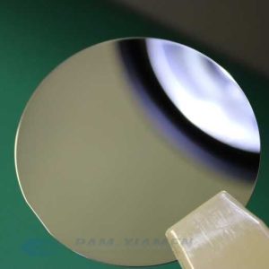
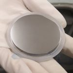
InP Wafer
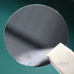
Indium phosphide (InP) is one of the important III-V compound semiconductors. It has the advantages of high electron mobility, good radiation resistance, and high band gap, which means that this material can amplify higher frequencies or signals with shorter wavelengths. Therefore, satellite receivers and amplifiers made of indium phosphide chips can work at extremely high frequencies above 100 GHz with high stability. Compared with gallium arsenide semiconductor materials, single crystal indium phosphide for sale from Ganwafer has a higher breakdown electric field and thermal conductivity, and higher electron mobility. More about our InP semiconductor wafer please see as follows:
- Description
- Inquiry
Description
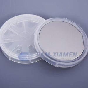
At present, the main sizes of InP single crystal substrates are 2-4 inches. From raw materials to ingots, indium phosphide is cut into a 2-inch or 4-inch wafer. The yield rate is generally about 28%, and the technical threshold is not generally high. The larger the indium phosphide wafer size, the higher the value.
1. Detail Specifications of Indium Phosphide Wafer
1.1. 4″ InP (Indium Phosphide) Single Crystal Wafer Specification
| Item | Specifications | |||
| Dopant | N-type | N-type | P-type | SI-type |
| Conduction Type | low doped | Sulphur | Zinc | lron |
| Wafer Diameter | 4″ | |||
| Wafer Orientation | (100)±0.5° | |||
| Wafer Thickness | 600±25um | |||
| Primary Flat Length | 16±2mm | |||
| Secondary Flat Length | 8±1mm | |||
| Carrier Concentration | ≤3x1016cm-3 | (0.8-6)x1018cm-3 | (0.6-6)x1018cm-3 | N/A |
| Mobility | (3.5-4)x103cm2/V.s | (1.5-3.5)x103cm2/V.s | 50-70x103cm2/V.s | >1000cm2/V.s |
| Resistivity | N/A | N/A | N/A | N/A |
| EPD | <1000cm-2 | <500cm-2 | <1x103cm-2 | <5x103cm-2 |
| TTV | <15um | |||
| BOW | <15um | |||
| WARP | <15um | |||
| Laser marking | upon request | |||
| Suface finish | P/E, P/P | |||
| Epi ready | yes | |||
| Package | Single wafer container or cassette | |||
1.2. 3″ Indium Phosphide Wafer Substrate Specification
| Item | Specifications | |||
| Dopant | N-type | N-type | P-type | SI-type |
| Conduction Type | low doped | Sulphur | Zinc | lron |
| Wafer Diameter | 3″ | |||
| Wafer Orientation | (100)±0.5° | |||
| Wafer Thickness | 600±25um | |||
| Primary Flat Length | 16±2mm | |||
| Secondary Flat Length | 8±1mm | |||
| Carrier Concentration | ≤3x1016cm-3 | (0.8-6)x1018cm-3 | (0.6-6)x1018cm-3 | N/A |
| Mobility | (3.5-4)x103cm2/V.s | (1.5-3.5)x103cm2/V.s | 50-70x103cm2/V.s | >1000cm2/V.s |
| Resistivity | N/A | N/A | N/A | N/A |
| EPD | <1000cm-2 | <500cm-2 | <1x103cm-2 | <5x103cm-2 |
| TTV | <12um | |||
| BOW | <12um | |||
| WARP | <15um | |||
| Laser marking | upon request | |||
| Suface finish | P/E, P/P | |||
| Epi ready | yes | |||
| Package | Single wafer container or cassette | |||
1.3. 2″ InP Wafer Substrate Specification
| Item | Specifications | |||
| Dopant | N-type | N-type | P-type | SI-type |
| Conduction Type | low doped | Sulphur | Zinc | lron |
| Wafer Diameter | 2″ | |||
| Wafer Orientation | (100)±0.5° | |||
| Wafer Thickness | 350±25um | |||
| Primary Flat Length | 16±2mm | |||
| Secondary Flat Length | 8±1mm | |||
| Carrier Concentration | 3x1016cm-3 | (0.8-6)x1018cm-3 | (0.6-6)x1018cm-3 | N/A |
| Mobility | (3.5-4)x103cm2/V.s | (1.5-3.5)x103cm2/V.s | 50-70x103cm2/V.s | >1000cm2/V.s |
| Resistivity | N/A | N/A | N/A | N/A |
| EPD | <1000cm-2 | <500cm-2 | <1x103cm-2 | <5x103cm-2 |
| TTV | <10um | |||
| BOW | <10um | |||
| WARP | <12um | |||
| Laser marking | upon request | |||
| Suface finish | P/E, P/P | |||
| Epi ready | yes | |||
| Package | Single wafer container or cassette | |||
2. Classification and Application of Indium Phosphide
According to conductivity performance, InP substrates are mainly divided into semi-conductive and semi-insulating substrates.
Semiconductor substrates are classified into N-type and P-type semiconducting substrates. Usually In2S3 and Sn are used as dopants for N-type substrates, and ZnP2 is used as dopants for p-type substrates. The purpose of the use of various dopants is to provide substrates of different conductivity types for device manufacturing, specifically as follows:
* N-type S-doped InP is not only used for laser diodes, but also for photodetectors. In order to avoid leakage current generated by dislocations, dislocation-free indium phosphide semiconductor doped with S is necessary. Because sulfur has an obvious impurity hardening effect in InP substrate, dislocation-free indium phosphide bulk single crystals are easy to grow.
* P-type Zn-doped indium phosphide (InP) is mainly used for high-power laser diodes. Zn also has a strong impurity hardening effect, so it can also make the dislocation ratio low. Low dislocation is very important to improve the life of the laser.
* Semi-insulating InP substrates are classified into doped semi-insulating substrates and non-doped semi-insulating substrates according to whether they are doped or not. Doped semi-insulating substrates usually use Fe2P as the dopant. The non-doped semi-insulating substrate is made of high-purity InP single crystal substrate through high-temperature annealing. Semi-insulating indium phosphide semiconductor substrates are mainly used to make radio frequency devices.