Who Are Ganwafer?
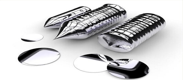
ガンウェーハは、半導体の結晶成長、プロセス開発、エピタキシーを統合した化合物半導体材料のトップクラスの企業です。 SiC&GaN材料(SiCウェーハとエピタキシー、GaNウェーハとエピウェーハ)およびIII-V材料(III-V基板とエピサービス:InPウェーハ、GaSbウェーハ、GaAsウェーハ、 InAsウェーハ、InSbウェーハ)。
主要な研究および製造会社として、1990年からCZシリコンウェーハおよびインゴットの研究と作成に専念し、1000ohm.cmを超えるFZシリコンウェーハを開発しています。 プライムグレードとテストグレードで2インチから12インチのウェーハサイズを提供できます。
Semiconductor wafers from Ganwafer are used in various applications. They are hugely used in LED semiconductor lighting, wireless communication, solar power, infrared device, laser, detectors, and semiconductor power devices, including power devices, high-temperature devices, and photoelectric devices, therein, GaN wafer including GaN on Si, GaN on SiC, and GaN on Sapphire are for Mini/micro LED, power electronics and microwave RF.
Why Ganwafer?
私たちの強さ
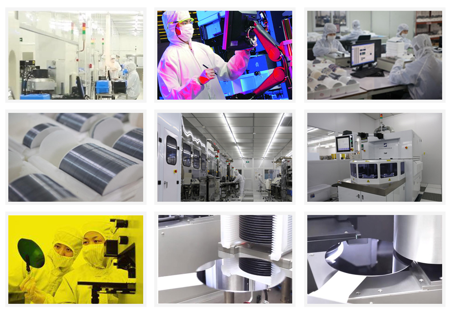
有名な主任研究員が率いる強力な技術研究開発チームの専門家チームがあり、強力な研究開発力を持っています。 私たちは、期待される製品を効果的に生産するためのトップウェーハファウンドリを持っています。 私たちの専門家は、新しい製品タイプの開発に役立つ市場動向に従って、最新の材料とデバイスをよく理解しています。 既存製品の品質を常に向上させることを目指しています。
高品質の製品
Ganwafer has been ISO9001:2015, owns and shares four modern foundries that able to deliver a range of industry-standard products with utmost quality. We ensure that our produced advanced wafer will meet clients’ needs, specifications, and budgets. We have been operating in this industry for many years that makes us stand out from the market. Each process of wafer manufacturing will be handled through our severe quality system. You can expect test reports for each shipment and each wafer are warranty.
25+年の経験
私たちは、材料の準備と関連機器の設計と開発、および材料の物理的、化学的、電気的特性、材料の準備手順に関する綿密な研究に豊富な経験を持っています。 理論的堆積に関する幅広い知識と科学技術者の実務経験は、当社のコアパワーです。
関連する材料と機器の拡張に関する長年の専門知識により、製品の品質と性能が向上します。 当社の機器設計スキームは、ユーザーの実際の技術的および技術的要件を満たすことができます。 当社の材料開発の豊富な歴史により、当社は市場から際立っており、さまざまな種類の化合物半導体の業界をリードする権威として、この業界のベンチマークを設定しています。
優れた品質
品質を損なうことなく業界標準に従って最高品質の製品を提供することが私たちの最優先事項です。 私たちは優れた顧客サービスを保証します。 私たちの営業担当者はあなたの質問をクリアし、ディストリビューターはスムーズな税関と輸送手順を確実にします。 私たちの尊敬するお客様は、手間をかけずに簡単に製品を購入できます。 顧客は予算の範囲内で手頃な価格の取引を受け取り、彼らのお金に対して最高の価値を得るでしょう。
グッド販売サービス
We understand that the requirements and specifications will vary with different clients and also the project size will vary. Do not bother at all! We are here to help you. We are capable enough to meet all of your requirements. Customers are free to ask their queries whatever they want to consult with our expert sales team. We ensure sustained and profitable growth for every customer, industry-standard products, and superior customer service.
私たちの歴史
市販のCdZnTe(CZT)ウェーハは、放射線を電子に効果的に変換できる新しい半導体である大量生産が行われており、主に赤外線薄膜エピタキシー基板、X線およびγ線検出、レーザー光変調に使用されます。 、高性能ソーラーセルおよびその他のハイテク分野。
Ganwafer has established the manufacturing technology for GaN epitaxy on Sapphire and freestanding GaN single crystal wafer substrate which is for UHB-LED and LD. Grown by hydride vapour phase epitaxy (HVPE) technology,Our GaN wafer has low defect density and less or free macro defect density.
Ganwafer develops and manufactures compound semiconductor substrates-gallium arsenide crystal and wafer.We has used advanced crystal growth technology,vertical gradient freeze (VGF) and GaAs wafer processing technology,established a production line from crystal growth, cutting, grinding to polishing processing and built a 100-class clean room for wafer cleaning and packaging. Our GaAs wafer include 2~6 inch ingot/wafers for LED,LD and Microelectronics applications.Thanks to its mastery of molecular beam epitaxy technology (MBE) and Metal Organic Chemical Vapor Deposition(MOCVD),the company can offer world class epitaxial compound semiconductor wafers for microwaves and RF applications.
Ganwafer has developed SiC crystal growth technology and SiC wafer processing technology, established a production line to manufacturer SiC substrate of polytype 4H and 6H in different quality grades for researcher and industry manufacturers,Which is applied in GaN epitaxy device,power devices, high-temperature device and optoelectronic Devices.As a professional company invested by the leading manufacturers from the fields of advanced and high-tech material research and state institutes and China’s Semiconductor Lab,we are devoted to continuously improve the quality of currently substates and develop large size substrates, as well as epitaxial technology.
Ganwafer has established production line of semiconductor materials – Ge(Germanium) Single Crystals and Wafers.
Ganwafer founded. Ganwafer develops advanced crystal growth and epitaxy technologies, manufacturing processes, engineered substrates and semiconductor devices.