
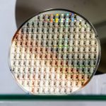
III-V Epi Wafer
High performance III-V semiconductor epi-structures are grown on GaAs, InP, GaSb, InAs, or InSb substrate. These different III-V epitaxial wafers are grown by MBE or MOCVD. Ganwafer, a leading III-V wafer foundry, supplies custom epi-structure to grow among compound semiconductor epitaxial stacks to meet customer demands. Please contact us for more information.
- Description
- Inquiry
Description
1. Photonic Technologiesfor III-V Materials and Device Growth
1.1 VCSEL Epitaxial Wafer
VCSEL (vertical cavity surface emitting laser) epi-structure is based on GaAs semiconductor material. Different from other light sources such as LED (light emitting diode) and LD (laser diode), the VCSEL structure has the advantages of small volume, circular output spot, single longitudinal mode output, small threshold current, low price and easy integration into large area array, which is widely used in optical communication, optical interconnection, optical storage and other fields. With the advantages of accuracy, miniaturization, low power consumption and reliability, 3D sensing camera with VCSEL chip as the core component will be widely used in mobile phones and other consumer electronic products.
We provide 4 and 6 inch GaAs based 650nm/680nm/795nm/850nm/905nm/940nm VCSEL’s layers stack wafer, primarily used for optical communication, LIDAR (self-driving cars), 3D sensing (mobile phones).
1.2 LD III-V Epitaxial Wafer
GaAs 808nm / 9xxnm semiconductor III-V epitaxy laser is used for industrial welding, marking, medical treatment, ranging, etc, including following III-V quantum dot laser material systems:
* InGaAs/GaAs/AlGaAs Laser:
Threshold current density < 75 A/cm 2 (980nm)
* InGaAsP/InP Laser:
Threshold current density < 200 mA/cm 2;
PL mapping uniformity <5 nm;
The slope efficiency > 0.35 W/A
* InGaAsSb/AlGaAsSb Laser:
Threshold current density < 200A/cm2 (2um, CW @ RT)
1.3 LED Epi Wafer
RCLED Wafer: a new type of LED structure. It is mainly composed of upper DBR (Bragg mirror), lower DBR and multiple quantum well (MQW) Active area composition, which has the advantages of both traditional LED and VCSEL. This epitaxial growth of III-V semiconductor is mostly used in optical fiber communication.
GaAs 650nm / 680nm / 795nm RCLED epitaxial wafer with advanced III-V structures: used for industrial sensors, atomic clocks, etc.
1.4 EEL Epitaxial Wafer
An edge emitting light emitting laser is presented. Its light emitting region is limited to a small part of one side. The limited light emitting region can improve the coupling efficiency with optical fiber and integrated optical path. Its working principle is to realize the non-equilibrium carrier number inversion between the energy band (conduction band and valence band) of semiconductor material, or between the energy band of semiconductor material and the impurity (acceptor or donor) energy level through a certain excitation mode. When a large number of electrons in the state of particle number inversion are combined with holes, stimulated emission will occur.
We provide 3, 4 and 6 inch GaAs based 808nm, 9XX nm, 980nm EEL epi-wafers, primarily used for industrial welding, lithography, medical applications, distance measurement.
1.5 Detector Epitaxy
We provide customized design of wafer scale III-V epilayers for PIN and APD:
InP 1.3um/1.5um laser and detector (pin, APD) epitaxial chip: used for optical communication, etc.
III-V wafer based APD chip
InGaAs PIN PD Chip
InGaAs APD Chip
InGaAs MPD Chip
GaAs PIN PD Chip
1.6 III-V Epi-Layer for Hall Sensor or Hall Device
InAs/GaAs Hall sensor:
Mobility > 20000 cm 2 / (V·s) @ 300K
InSb/GaAs Hall device:
Mobility > 60000 cm 2 / (V·s) @ 300K
2. III-V Epitaxy for Power & RF Technologies
2.1 HEMT Wafer on III-V Group Semiconductor
HEMT is a kind of heterojunction field effect transistor, also known as modulation doped field effect transistor (MODFET), two-dimensional electron gas field effect transistor (2degfet), selective doped heterojunction transistor (SDHT), etc. This device and its integrated circuit can work in the field of ultra-high frequency (millimeter wave) and ultra-high speed, because it works by using the so-called two-dimensional electron gas with high mobility. The basic structure of HEMT is a modulation doped heterojunction. Two dimensional electron gas (2DEG) with high mobility exists in modulation doped heterostructures. This kind of 2DEG not only has high mobility, but also does not “freeze” at very low temperature. Therefore, HEMT based on III-V technologies has good low temperature performance and can be used in low temperature research.
GaAs/AlGaAs HEMT:
Mobility > 7000 cm 2 / (V·s) @ RT
2.2 III-V Semiconductor based pHEMT Wafer
pHEMT is an improved structure of HEMT, PHEMT has a double heterojunction structure, which not only improves the temperature stability of the device threshold voltage, but also improves the output volt ampere characteristics of the device, making the device have larger output resistance, higher transconductance, greater current processing capacity, higher operating frequency and lower noise.
The 2DEG in pHEMT is more limited than that in ordinary HEMT (with double confinement on both sides of the well), so it has higher electron surface density (about 2 times higher); at the same time, the electron mobility here is also higher (9% higher than that in GaAs), so the performance of pHEMT is better.
For more pHEMT wafer specifications, please view:
Si-Delta Doped GaAs PHEMT Heterostructure
2.3 mHEMT Wafer with III-V Quantum Well
GaAs based InAlAs / InGaAs large mismatch mHEMT combines the advantages of high frequency, high power gain and low noise figure of InP based HEMT, as well as the advantages of mature GaAs based HEMT III-V epi wafer manufacturing process, showing good application potential in millimeter wave band.
2.4 MESFET Wafer Epitaxy with III-V Nanostructure
GaAs MESFET epi growth wafer has excellent microwave, high speed, high power and low noise performance. For example, the noise of microwave GaAs MESFET with gate length L = 1 μ m and gate width W = 250 μ m is 1 dB (corresponding BJT is 2 dB) in C band and 2.5 ~ 3 dB (corresponding BJT is 5 dB) in Ku band. Compared with microwave silicon BJT, GaAs MESFET not only has high operating frequency (up to 60GHz), low noise, but also high saturation level and high reliability. This is due to the fact that the electron mobility of n-GaAs epitaxial material is 5 times larger and the peak drift speed is 2 times larger than that of silicon, and the substrate of the device can be semi insulating GaAs (Si GaAs) to reduce the parasitic capacitance.
2.5 HBT Epitaxial Wafer
HBT epi wafer grown with group III-V semiconductors can be used in 5G wireless communication technology and optical fiber communication technology.
3. Group III-V Wafer for Solar Technologies
We are running GaInP/GaAs/Ge or GaAs III-V epitaxy with triple-junction cells.
Thanks to GaAs tunnel junction technology, our III-V wafer foundry can offer single-junction, dual-junction and Triple-junction multilayer epitaxy for solar cell fabricated by a MOCVD technique and made of high-quality III-V compounds materials that deliver significantly high efficiency. Compared with conventional solar cells, multi-junction solar cells are more efficient but also more expensive to manufacture. Triple-junction cells are more cost effective. The III-V epi wafer for sale is used in space applications.
Remark:
The Chinese government has announced new limits on the exportation of Gallium materials (such as GaAs, GaN, Ga2O3, GaP, InGaAs, and GaSb) and Germanium materials used to make semiconductor chips. From August 1, 2023 on, exporting these materials is only allowed if we obtains a license from the Chinese Ministry of Commerce. Hope for your understanding!