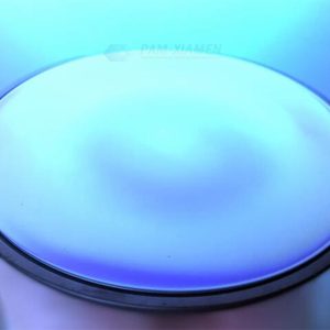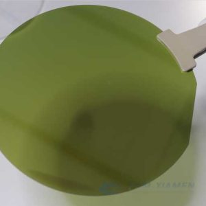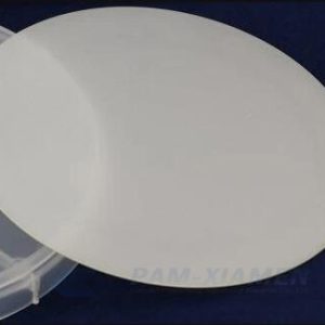
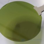
GaN on Sapphire HEMT Wafer

Ganwafer offers GaN on Sapphire wafers with HEMT structure and GaN template on Sapphire substrate for power or RF devices. The epitaxial layers of GaN based materials and devices are mainly grown on sapphire substrates. Why epitaxial GaN growth on Sapphire? Reasons are that sapphire substrate has many advantages: firstly, sapphire substrate has mature production technology and good device quality; secondly, sapphire has good stability and can be used in high temperature growth process; finally, sapphire has high mechanical strength and is easy to handle and clean. Therefore, most of the GaN HEMT wafer processes are based on sapphire. However, using sapphire as substrate also has some problems, such as lattice mismatch and thermal stress mismatch, which will produce a large number of defects in the GaN / Sapphire epitaxial layer and cause difficulties in the subsequent device processing.
And now please see below GaN-on-Sapphire HEMT wafer specifications:
- Description
- Inquiry
Description
1. GaN on Sapphire Wafer with HEMT Structure for Power Application
| Wafer size | 2”, 3”, 4”, 6” |
| AlGaN/GaN HEMT structure | Refer 1.2 |
| Carrier density | 6E12~2E13 cm2 |
| Hall mobility | / |
| XRD(102)FWHM | ~arc.sec |
| XRD(002)FWHM | ~arc.sec |
| Sheet Resistivity | / |
| AFM RMS (nm)of 5x5um2 | <0.25nm |
| Bow(um) | <=35um |
| Edge exclusion | <2mm |
| SiN passivation layer | 0~30nm |
| Al composition | 20-30% |
| In composition | 17% for InAlN |
| GaN cap | / |
| AlGaN/(In)AlN barrier | / |
| AlN interlayer | / |
| GaN channel | / |
| C doped GaN buffer | / |
| Nudeation | / |
| Substrate material | Sapphire substrate |
2. GaN HEMT Structure on Sapphire Substrate for RF Application
| Wafer size | 2”, 3”, 4”, 6” |
| AlGaN/GaN HEMT structure | Refer 1.2 |
| Carrier density | 6E12~2E13 cm2 |
| Hall mobility | / |
| XRD(102)FWHM | / |
| XRD(002)FWHM | / |
| Sheet Resistivity | / |
| AFM RMS (nm)of 5x5um2 | <0.25nm |
| Bow(um) | <=35um |
| Edge exclusion | <2mm |
| siN passivation layer | 0~30nm |
| u-GaN cap layer | / |
| Al composition | 20-30% |
| In composition | 17% for InAlN |
| AlGaN barrier layer | 20~30nm |
| AlN spacer | / |
| GaN buffer layer(um) | / |
| GaN channel | / |
| Fe doped GaN buffer | / |
| Nudeation | / |
| Substrate material | Sapphire substrate |
Remark:
The Chinese government has announced new limits on the exportation of Gallium materials (such as GaAs, GaN, Ga2O3, GaP, InGaAs, and GaSb) and Germanium materials used to make semiconductor chips. From August 1, 2023 on, exporting these materials is only allowed if we obtains a license from the Chinese Ministry of Commerce. Hope for your understanding!