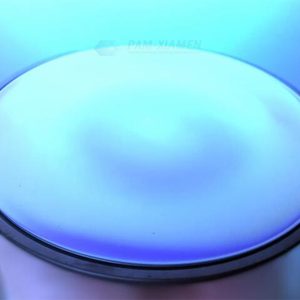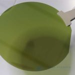
GaN on SiC HEMT Wafer
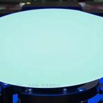
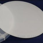
Ganwafer offers GaN on SiC (Silicon Carbide) HEMT Wafer and GaN on SiC epitaxy template.
Because the thermal conductivity of silicon carbide is much higher than that of GaN, Si and sapphire, the lattice mismatch between SiC and GaN is very small. SiC substrate can improve the heat dissipation characteristics and reduce the junction temperature of the device. However, the wettability of GaN and SiC is poor, so it is difficult to obtain smooth GaN epitaxial growth on SiC substrate. The migration activity of AlN on SiC matrix is small and the wettability with SiC matrix is good. Therefore, AlN is usually used as the nucleation layer of GaN on SiC wafer to improve GaN crystal quality by optimizing the growth conditions of AlN nucleation layer. Due to the small lattice mismatch, once the wetting layer and crack problems are solved by our GaN on SiC process technology, the quality of GaN on silicon carbide substrate is better than that on Si and sapphire substrate. Therefore, the transport performance of GaN heterostructure 2DEG on SiC substrate is better.
GaN on SiC HEMT wafer specification:
- Description
- Inquiry
Description
1. AlGaN / GaN-on-SiC HEMT Wafer for RF Application
| Wafer size | 2”, 3”, 4”, 6” |
| AlGaN/GaN HEMT structure | Refer 1.2 |
| Carrier density | 6E12~2E13 cm2 |
| Hall mobility | 1300~2200 cm2v-1s-1 |
| XRD(102)FWHM | <300arc.sec |
| XRD(002)FWHM | <260arc.sec |
| Sheet Resistivity | 200~450 ohm/sq |
| AFM RMS (nm)of 5x5um2 | <0.25nm |
| Bow(um) | <=35um |
| Edge exclusion | <2mm |
| SiN passivation layer | 0~30nm |
| GaN cap layer | 2nm |
| Al composition | 20-30% |
| In composition | 17% for InAlN |
| AlGaN | / |
| AlN interlayer | / |
| GaN channel | / |
| Fe doped GaN buffer | 1.6um |
| AlN buffer layer | / |
| Substrate material | SiC Substrate |
2. Specification of GaN on SiC Template
2″ or 4” GaN on 4H or 6H SiC substrate
| 1) Undoped GaN buffer or AlN buffer are available; | ||||
| 2) n-type(Si doped or undoped), p-type or semi-insulating GaN epitaxial layers available; | ||||
| 3) Vertical conductive structures on n-type or semi-insulating SiC; | ||||
| 4) AlGaN – 20-60nm thick, (20%-30%Al), Si doped buffer; | ||||
| 5) GaN n-type layer on 350µm+/-25um thick 2” or 4” wafer. | ||||
| 6) Single or double side polished, epi-ready, Ra<0.5um | ||||
| 7) Typical value on XRD: | ||||
| Wafer ID | Substrate ID | XRD(102) | XRD(002) | Thickness |
| #2153 | X-70105033 (with AlN) | 298 | 167 | 679um |
Remark:
The Chinese government has announced new limits on the exportation of Gallium materials (such as GaAs, GaN, Ga2O3, GaP, InGaAs, and GaSb) and Germanium materials used to make semiconductor chips. From August 1, 2023 on, exporting these materials is only allowed if we obtains a license from the Chinese Ministry of Commerce. Hope for your understanding!