LED Epi on GaAs Substrate

Gallium arsenide (GaAs) occupies a large part in the field of optoelectronic lasers and LEDs. As mature second-generation compound semiconductors, power chips and optoelectronic chips both grow different material film structures on GaAs substrates by means of epitaxial growth.
The minimum conduction band and maximum valence band of GaAs are located at k=0, which means that electrons in GaAs can directly reach the top of the valence band from the bottom of the conduction band when the electron transitions. Compared with silicon, electrons only need a change in energy during the transition from the conduction band to the valence band, but the momentum does not change. This property gives GaAs a unique advantage in the manufacture of semiconductor lasers (LD) and light-emitting diodes (LED).
- Description
- Inquiry
Description
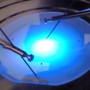
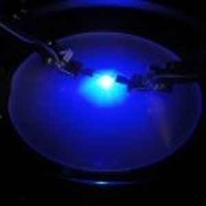
Ganwafer offers LED Epi wafer on GaAs substrate, which is grown by MOCVD, available wavelength are:
Red: 630~650nm;
Yellow: 587 ~ 592nm;
Yellow / Green: 568 ~ 573nm;
Infrared: 810~880nm, 890~940nm.
More specifications of GaAs LED epitaxy please see below:
1. Red LED Epi on GaAs Substrate
1.1 Positive Structure of Red LED Wafer
| Structure | Thickness(nm) |
| P-GaP | – |
| P-AlInP | – |
| MQW | – |
| N-AlInP | – |
| DBR n-AlGaAs/AlAs | – |
| Buffer layer n-GaAs | – |
| GaAs Substrate | 350um |
1.2 Reverse Polarity Structure of Red LED Wafer
| Structure | Thickness(nm) |
| C-GaP | – |
| Mg-GaP | – |
| Mg-AlGaInP | – |
| Mg-AlInP | – |
| AlInP | – |
| MQW:AlGaInP | – |
| Si-AlInP | – |
| Si-Al0.6GaInP | – |
| Si-GaInP | – |
| Si-GaAs ohm contact layer | – |
| Si-GaInP etching layer | – |
| Si-GaAs buffer | – |
| GaAs substrate | 350um |
Mark: We also can grow the LED epitaxial structure on 625 +/- 50 um thick GaAs substrate, and the wafer size can reach 100 mm. The actual wavelength has a tolerance at +/-10.
2. RC LED Epi Layer on GaAs Substrate, 650nm
| P+ GaP 100nm (For ITO) |
| P GaP 2um |
| P AlGaAs/AlAs DBR X 10 |
| P AllnP |
| I AlGaInp MQW |
| N AllnP |
| N AlGaAs/AlAs DBRX30 |
| N GaAs buffer |
| N-GaAs substrate (15degree off) |
3. Infrared LED Epitaxial on GaAs Substrate, 850-870nm
| Material | Type | Thickness(nm) | note |
| AlGaAs | P+ | – | ohmiccontact layer |
| AlGaAs | P | – | P-Cladding |
| AlGaAs/GaAs | undoped | – | Active layer |
| AlGaAs | N | – | N-Cladding |
| N-GaAs substrate | |||
4. FAQ for Infrared LED Epi on GaAs Substrate
Q1: Is it possible to modify some thicknesses of the 1.2 Reverse Polarity Structure of Red LED Wafer? For example, increasing the etch stop layer to 300 nm.
A: Yes, etch stop layer of the IR LED structure can do 300 nm.
Q2: For the LED epitaxy structure in 1.2, are you able to tell me some doping information, specifically around the contact? It would be very helpful so we can properly design metal contacts.
A: For contact layer of LED epi-structure, the n doping should be ~2e18, and the p doping in the contact layer should be ~1e20.
Q3: How do you typically make contact to the GaP:C p-contact layer in Reverse Polarity LED Structure? For example, ITO or Ti/Pt/Au?
A: Usually we use ITO as contact for the LED wafer.
Q4:Is the DBR n-AlGaAs/AlAs layer in positive LED wafer working as a reflector/mirror designed for the emission wavelength?
A: Yes, the DBR n-AlGaAs/AlAs layer in GaAs LED positive wafer is worked as a reflector/mirror.
Q5: Does the Si-Al0.6GaInP layer in reverse polarity structure of GaAs LED epitaxy also works as a reflector/mirror?
A:Yes, the Si-Al0.6GaInP epilayer in reversed GaAs LED epi-structure works as reflector/mirror.
Remark:
The Chinese government has announced new limits on the exportation of Gallium materials (such as GaAs, GaN, Ga2O3, GaP, InGaAs, and GaSb) and Germanium materials used to make semiconductor chips. From August 1, 2023 on, exporting these materials is only allowed if we obtains a license from the Chinese Ministry of Commerce. Hope for your understanding!