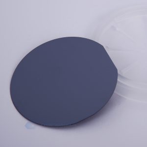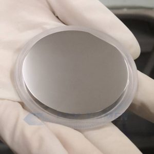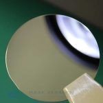
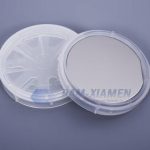
InSb Wafer
Indium antimonide (InSb) has the highest electron mobility and saturation speed among all semiconductors, so it can be used in low power consumption and extremely high frequency devices. As a manufacturer of compound semiconductor InSb wafer, Ganwafer provide LEC grown III-V group indium antimonide substrates
There are many potential applications of indium antimonide compound wafer due to its low crystallization temperature, narrow band gap, high carrier mobility, relatively simple high-purity indium antimonide single crystal process, complete indium antimonide crystal structure, and good electrical parameter uniformity. Indium antimonide wafer is currently used in field effect transistors (FETs), making the digital device low power consumption and fast response. More about the indium antimony wafer please contact us.
- Description
- Inquiry
Description
Single crystal epi-ready indium antimonide wafers are still one of the main semiconductors used for the fabrication of electronic components for solid state electronics. The InSb wafer is used for the fabrication of linear and array photocells operated in the wavelength of 3–5mm, and used as photosensitive elements in heat vision systems.
Moreover, focal arrays based on indium antimonide thin films are used as special devices for airborne navigation and precision targeting systems, antiaircraft infrared tracking heads, marine infrared detectors and etc.
1. InSb Wafer Specifications
| Item | Specifications |
| Wafer Diameter | 2″50.5±0.5mm 3″76.2±0.4mm 4″1000.0±0.5mm |
| Crystal Orientation | 2″(111)AorB±0.1° 3″(111)AorB±0.1° 4″(111)AorB±0.1° |
| Thickness | 2″625±25um 3″ 800or900±25um 4″1000±25um |
| Primary flat length | 2″16±2mm 3″22±2mm 4″32.5±2.5mm |
| Secondary flat length | 2″8±1mm 3″11±1mm 4″18±1mm |
| Surface Finish | P/E, P/P |
| Package | Epi-Ready,Single wafer container or CF cassette |
2.Electrical and Doping Parameters of N-type and P-type Indium Antimonide Wafer
| Conduction Type | n-type | n-type | n-type | n-type | p-type |
| Dopant | low doped | Tellurium | Low tellurium | High tellurium | Genmanium |
| EPD cm-2 | 2″3″4″≤50 | 2″≤100 | |||
| Mobility cm² V-1s-1 | ≥4*105 | ≥2.5*104 | ≥2.5*105 | Not Specified | 8000-4000 |
| Carrier Concentration cm-3 | 5*1013-3*1014 | (1-7)*1017 | 4*1014-2*1015 | ≥1*1018 | 5*1014-3*1015 |
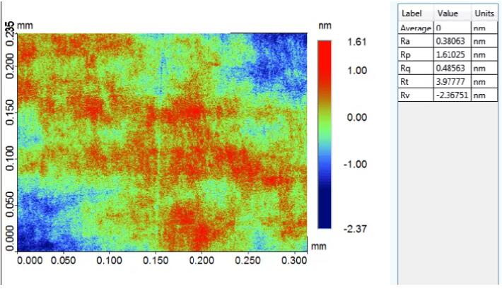
3. Research on Chemical Polishing of InSb Wafer
Mechanical polishing will cause mechanical damage to the surface of the InSb wafer to a certain extent, increase the surface roughness of the wafer, and affect the performance of the final device. The chemical polishing can remove the surface scratches of the InSb substrate and reduce the surface roughness. The n-type or p-type indium antimonide substrate is mechanically polished and further polished with a low concentration Br_2-MeOH solution. Compare the topography, total thickness variation (TTV), roughness, surface composition and impurities of polished and unpolished InSb wafers, the results show that when polishing InSb wafers with a low concentration of Br_2-MeOH solution, the corrosion rate is stable, easy to control, and can effectively remove surface scratches and obtain a smooth mirror surface. The surface roughness of the wafer after chemical polishing is 6.443nm, TTV is 3.4μm, and the atomic ratio of In/Sb is close to 1. Compared with the traditional CP4-A and CP4-B etching solutions, the low concentration Br_2-MeOH solution is more suitable for chemical polishing of InSb wafers.