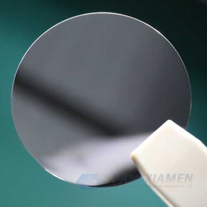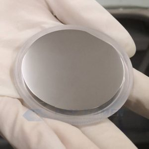
GaSb Wafer
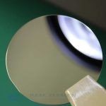
Gallium antimonide (GaSb) material from Ganwafer a gallium antimonide wafer supplier is an important substrate material for manufacturing 2~4um lasers, infrared light-emitting tubes and high-speed low-noise avalanche photodiodes. Its three- and quaternary compound epitaxial growth has good lattice matching, and it is one of the ideal light source materials for manufacturing optical communication devices. Device manufacturing on single crystal GaSb substrate requires the preparation of a stable oxide layer with low interface density, high resistivity, high breakdown voltage and suitable for high-temperature processes. More about GaSb (Gallium Antimonide) crystal substrates please contact us.
- Description
- Inquiry
Description
As one of important III–V compound semiconductor materials, gallium antimonide is applied in optoelectronic devices. Because of the gallium antimonide properties, such as high quantum efficiency, high hole mobility, and super lattices with customized optical and transport characteristics, devices fabricated on GaSb substrate is ideal for the mid-infrared (2-5um and 8-14um wavelength) applications, like imaging sensors for fire detection, surveillance system and environmental pollution monitors.
1. 4″ Epitaxy-ready GaSb Wafer Specification
| Item | Specifications | ||
| Dopant | low doped | Zinc | Tellurium |
| Conduction Type | P-type | P-type | N-type |
| Wafer Diameter | 4″ | ||
| Wafer Orientation | (100)±0.5° | ||
| Wafer Thickness | 800±25um | ||
| Primary Flat Length | 32.5±2.5mm | ||
| Secondary Flat Length | 18±1mm | ||
| Carrier Concentration | (1-2)x1017cm-3 | (5-100)x1017cm-3 | (1-20)x1017cm-3 |
| Mobility | 600-700cm2/V.s | 200-500cm2/V.s | 2000-3500cm2/V.s |
| EPD | <2×103cm-2 | ||
| TTV | <15um | ||
| BOW | <15um | ||
| WARP | <20um | ||
| Laser marking | upon request | ||
| Surface finish | P/E, P/P | ||
| Epi ready | yes | ||
| Package | Single wafer container or cassette | ||
2. 3″ Gallium Antimonide Wafer Specification
| Item | Specifications | ||
| Conduction Type | P-type | P-type | N-type |
| Dopant | low doped | Zinc | Tellurium |
| Wafer Diameter | 3″ | ||
| Wafer Orientation | (100)±0.5° | ||
| Wafer Thickness | 600±25um | ||
| Primary Flat Length | 22±2mm | ||
| Secondary Flat Length | 11±1mm | ||
| Carrier Concentration | (1-2)x1017cm-3 | (5-100)x1017cm-3 | (1-20)x1017cm-3 |
| Mobility | 600-700cm2/V.s | 200-500cm2/V.s | 2000-3500cm2/V.s |
| EPD | <2×103cm-2 | ||
| TTV | <12um | ||
| BOW | <12um | ||
| WARP | <15um | ||
| Laser marking | upon request | ||
| Surface finish | P/E, P/P | ||
| Epi ready | yes | ||
| Package | Single wafer container or cassette | ||
3. 2″ GaSb (Gallium Antimonide) Wafer Substrate Specification
| Item | Specifications | ||
| Dopant | low doped | Zinc | Tellurium |
| Conduction Type | P-type | P-type | N-type |
| Wafer Diameter | 2″ | ||
| Wafer Orientation | (100)±0.5° | ||
| Wafer Thickness | 500±25um | ||
| Primary Flat Length | 16±2mm | ||
| Secondary Flat Length | 8±1mm | ||
| Carrier Concentration | (1-2)x1017cm-3 | (5-100)x1017cm-3 | (1-20)x1017cm-3 |
| Mobility | 600-700cm2/V.s | 200-500cm2/V.s | 2000-3500cm2/V.s |
| EPD | <2×103cm-2 | ||
| TTV | <10um | ||
| BOW | <10um | ||
| WARP | <12um | ||
| Laser Marking | upon request | ||
| Surface Finish | P/E, P/P | ||
| Epi Ready | yes | ||
| Package | Single wafer container or cassette | ||
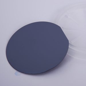
Many semiconductor device characteristics are closely related to characteristics of semiconductor surface. It is worth noting that single crystal GaSb wafer is easy to oxide by atmospheric oxygen formed natural surface oxides with a few nanometers thick since it has a very high chemically reactive surface.
Remark:
The Chinese government has announced new limits on the exportation of Gallium materials (such as GaAs, GaN, Ga2O3, GaP, InGaAs, and GaSb) and Germanium materials used to make semiconductor chips. From August 1, 2023 on, exporting these materials is only allowed if we obtains a license from the Chinese Ministry of Commerce. Hope for your understanding!