P Type GaN on Sapphire or Silicon Template
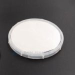
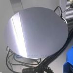
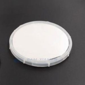
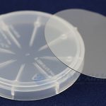
Ganwafer’s Template Products consist of crystalline layers of gallium nitride (GaN), which are deposited on sapphire/silicon(111) substrates. It includes P type/n type/ semi-insulating GaN/Sapphire or silicon template, available diameters from 2″ up to 6″,and consist of a thin layer of crystalline GaN grown on a sapphire/silicon substrate. Epi-ready templates now available.
- Description
- Inquiry
Description
1. Specifications of GaN on Sapphire Template
1.1 4 inch Mg-Doped GaN/Sapphire Substrates
| Item | GANW-T-GaN-100-P |
| Dimension | 100 ±0.1 mm |
| Thickness | 5 ±1 μm |
| Orientation of GaN | C plane (0001) off angle toward A-axis 0.2 ±0.1° |
| Orientation Flat of GaN | (1-100) 0 ±0.2°, 16 ±1 mm |
| Conduction Type | P-type |
| Resistivity (300K) | ~ 10 Ω·cm |
| Carrier Concentration | >6X10¹⁶CM-3(doping concentration≥10x1020cm-3 |
| Mobility | ~ 10cm2 / V·s |
| Dislocation Density | < 5x108cm-2(estimated by FWHMs of XRD) |
| Structure | 2~2.5 μm pGaN/2~2.5 μm pGaN uGaN/50nm uGaN buffer layer/430±25μm |
| Orientation of Sapphire | C plane (0001) off angle toward M-axis 0.2 ±0.1° |
| Orientation Flat of Sapphire | (11-20) 0 ±0.2°, 16 ±1 mm |
| Surface Roughness: | Front side: Ra<0.5nm, epi-ready; |
| Back side: etched or polished. | |
| Useable Area | > 90% (edge and macro defects exclusion) |
| Package | each in single wafer container, under nitrogen atmosphere, packed in class 100 clean room |
1.2 2 inch Mg-Doped GaN/Sapphire Substrates
| Item | GANW-T-GaN-50-P |
| Dimension | 50.8 ±0.1 mm |
| Thickness | 5 ±1 μm |
| Orientation of GaN | C plane (0001) off angle toward A-axis 0.2 ±0.1° |
| Orientation Flat of GaN | (1-100) 0 ±0.2°, 16 ±1 mm |
| Conduction Type | P-type |
| Resistivity (300K) | ~ 10 Ω·cm |
| Carrier Concentration | >6X10¹⁶CM-3(doping concentration≥10x1020cm-3 |
| Mobility | ~ 10cm2 / V·s |
| Dislocation Density | < 5x108cm-2(estimated by FWHMs of XRD) |
| Structure | 2~2.5 μm pGaN/2~2.5 μm pGaN uGaN/50nm uGaN buffer layer/430±25μm |
| Orientation of Sapphire | C plane (0001) off angle toward M-axis 0.2 ±0.1° |
| Orientation Flat of Sapphire | (11-20) 0 ±0.2°, 16 ±1 mm |
| Surface Roughness: | Front side: Ra<0.5nm, epi-ready; |
| Back side: etched or polished. | |
| Useable Area | > 90% (edge and macro defects exclusion) |
2. Specification of P Type GaN on Silicon Template
| Description | Type | Dopant | Substrate | Size | GaN thickness | Surface |
| GaN Template on 4″ Silicon Wafer, GaN film | P type | Mg doped | Si (111) substrates | 4″ | 2um | single side polished |
| GaN Template on 2″ Silicon Wafer, GaN film | P type | Mg doped | Si (111) substrates | 2″ | 2um | single side polished |
3. 2″ Dia, P Type GaN on Silicon
2 dia, GaN on silicon
GaN layer thickness : 2um
GaN layer: P type, Mg doped.
Structure:GaN on Silicon(111).
Substrate: Silicon(111), p type, 430+/-25um
XRD(102)<700arc.sec
XRD(002)<500arc.sec
Single Side Polished, Epi-ready,Ra<0.5nm
Carrier concentration:5E17~5E18
Remark:
The Chinese government has announced new limits on the exportation of Gallium materials (such as GaAs, GaN, Ga2O3, GaP, InGaAs, and GaSb) and Germanium materials used to make semiconductor chips. From August 1, 2023 on, exporting these materials is only allowed if we obtains a license from the Chinese Ministry of Commerce. Hope for your understanding!