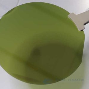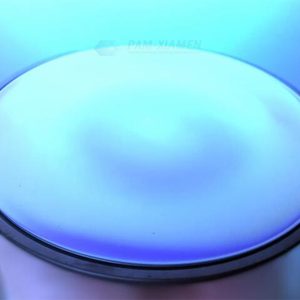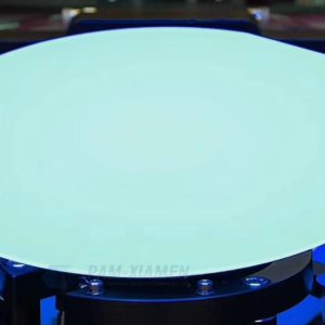
GaN on GaN
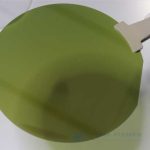
GaN (Gallium Nitride) on GaN wafer is the best solution because of zero lattice mismatch between substrate and epi layers. The lower defect in GaN / GaN film provides extended device durability. The lattice and thermal expansion coefficient of GaN-on-GaN wafer are perfectly matched. Therefore, a very thick GaN layer can be epitaxially grown on a bulk GaN substrate, enabling the fabrication of high breakdown voltage devices. Ganwafer, a GaN on GaN wafer manufacturer, offers 2” and 4” GaN on GaN epi wafer in wide bandgap (WBG) semiconductors:
- Description
- Inquiry
Description
1. N+ GaN Layers on N+ GaN Substrate
| Item 1 | Specifications |
| GaN wafer | 100 mm or 50.8mm,N+ GaN Wafer |
| 1Epi growth | N+,10-15um, Nd: 1E15-1E16 |
2. N+/P+ GaN Layers on N+ GaN Substrate
| Item 2 | Specifications |
| GaN wafer | 100 mm or 50.8mm,N+ GaN Wafer |
| 1Epi growth | N+, 10-15um,Nd:1E15-1E16 |
| 2Epi growth | 0.5-2um, P type, Na:1E17-1E19 |
| 3Epi growth | 0.1um, P type,GaN, Na:-8E19 |
3. N+GaN Layers on Semi-insulating GaN Substrate
| Item 3 | Specifications |
| GaN wafer | 100 mm or 50.8mm, Semi-insulating GaN Wafer |
| 1Epi growth | N+,10-15um,Nd:1E15-1E16 |
4. Vertical Technology of GaN/GaN Wafer
Vertical GaN technology takes the full use of GaN properties because it is based on homoepitaxial growth of GaN on a GaN substrate. The obvious features of vertical GaN technology:
Homoepitaxial growth on GaN substrate obtains the best spectra of these cut-in angles, resulting in the best morphology and the best device performance. Flexible use of bulk GaN substrate from can produce ultra-low-doped n-GaN. Controlling Mg doping is to grade p-n junctions during the growth process. Generating sharp pn junction as needed is a planarized regrowth process for surface roughness with extremely low surface roughness. In the case of vertical p GaN/n GaN, both the substrate and the epitaxial layer are GaN with extremely low defect density.
Remark:
The Chinese government has announced new limits on the exportation of Gallium materials (such as GaAs, GaN, Ga2O3, GaP, InGaAs, and GaSb) and Germanium materials used to make semiconductor chips. From August 1, 2023 on, exporting these materials is only allowed if we obtains a license from the Chinese Ministry of Commerce. Hope for your understanding!