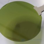
GaN su GaN
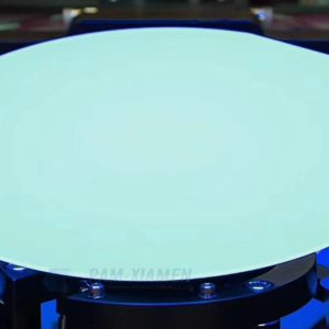
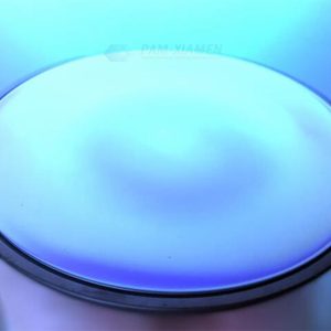
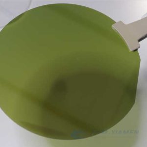
GaN (Gallium Nitride) on GaN wafer is the best solution because of zero lattice mismatch between substrate and epi layers. The lower defect in GaN / GaN film provides extended device durability. The lattice and thermal expansion coefficient of GaN-on-GaN wafer are perfectly matched. Therefore, a very thick GaN layer can be epitaxially grown on a bulk GaN substrate, enabling the fabrication of high breakdown voltage devices. Ganwafer, a GaN on GaN wafer manufacturer, offers 2” and 4” GaN on GaN epi wafer in wide bandgap (WBG) semiconductors:
- Descrizione
- Inchiesta
Descrizione
1. Strati N+ GaN su substrato N+ GaN
| Articolo 1 | Specificazioni |
| Wafer di GaN | Wafer da 100 mm o 50,8 mm,N+ GaN |
| 1Epi di crescita | N+,10-15um, Nd: 1E15-1E16 |
2. Strati N+/P+ GaN su substrato N+ GaN
| Articolo 2 | Specificazioni |
| Wafer di GaN | Wafer da 100 mm o 50,8 mm,N+ GaN |
| 1Epi di crescita | N+, 10-15um,Nd:1E15-1E16 |
| 2Epi di crescita | 0,5-2um, tipo P, Na:1E17-1E19 |
| Crescita 3Epi | 0,1 um, tipo P, GaN, Na:-8E19 |
3. Strati N+GaN su substrato GaN semiisolante
| Articolo 3 | Specificazioni |
| Wafer di GaN | Wafer semiisolante GaN da 100 mm o 50,8 mm |
| 1Epi di crescita | N+,10-15um,Nd:1E15-1E16 |
4. Tecnologia verticale del wafer GaN/GaN
La tecnologia GaN verticale sfrutta appieno le proprietà del GaN perché si basa sulla crescita omoepitassiale del GaN su un substrato di GaN. Le caratteristiche ovvie della tecnologia GaN verticale:
La crescita omoepitassiale sul substrato di GaN ottiene i migliori spettri di questi angoli di taglio, risultando nella migliore morfologia e nelle migliori prestazioni del dispositivo. L'uso flessibile del substrato GaN sfuso può produrre n-GaN a bassissimo drogaggio. Il controllo del doping da Mg consiste nel classificare le giunzioni pn durante il processo di crescita. La generazione di giunzione pn affilata secondo necessità è un processo di ricrescita planarizzata per rugosità superficiale con rugosità superficiale estremamente bassa. Nel caso di p GaN/n GaN verticale, sia il substrato che lo strato epitassiale sono GaN con densità di difetto estremamente bassa.
Remark:
The Chinese government has announced new limits on the exportation of Gallium materials (such as GaAs, GaN, Ga2O3, GaP, InGaAs, and GaSb) and Germanium materials used to make semiconductor chips. From August 1, 2023 on, exporting these materials is only allowed if we obtains a license from the Chinese Ministry of Commerce. Hope for your understanding!