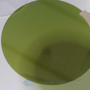
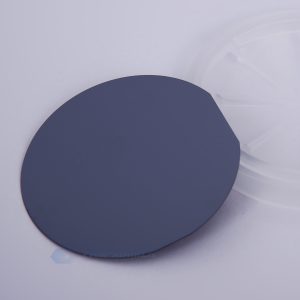
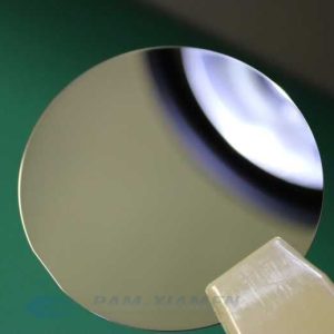
Ganwafer offers semiconductor wafer materials, including compound semiconductor wafer (such as GaSb, InAs, and InSb wafer), Germanium (Ge) wafer, and CdZnTe (CZT) wafer.
Informazioni sui wafer a semiconduttore
Un wafer semiconduttore è solitamente una pellicola sottile di sostanza semiconduttrice ampiamente utilizzata in elettronica per la realizzazione di circuiti integrati. Il semiconduttore epi wafer esiste come ASIC o IC in ogni dispositivo elettronico che utilizziamo.
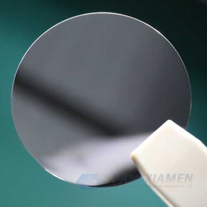
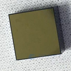
Semiconductor substrate and wafer are a round piece of wafer that consists of the wafer die that performs a very specific functionally. They are the basic material for manufacturing electronic chips. The basic semiconductor substrate wafer manufacturing process includes wafer growth, wafer cleaning and wafer packaging.
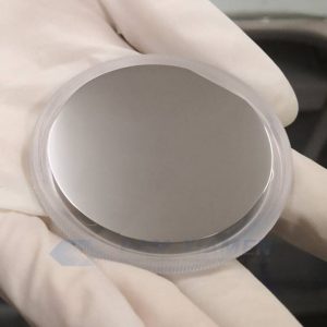
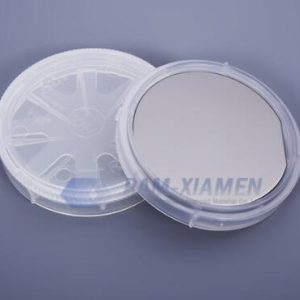
Ganwafer is one of a leading semiconductor wafer manufacturing companies that offers a wide range of wafers in different sizes in this case diameters. The semiconductor wafer size has increased throughout to reduce production costs in our semiconductor wafer foundry.
The thickness of semiconductor wafers can vary greatly. The thickness of a wafer is determined by the mechanical strength of any material used to make it. No matter how a wafer is made, the wafer layers must be thick enough to support its own weight so as not to break during processing.