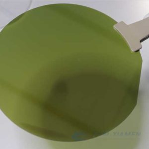
GaN su wafer HEMT di silicio
Ganwafer offers GaN (Gallium Nitride) on Silicon (Si) Epitaxy HEMT wafer and GaN template on Si substrate. According to different applications, GaN on Silicon HEMT wafer can be classified into GaN-on-Silicon wafer for D-mode, GaN on Silicon substrate for E-mode and GaN on Silicon wafer for RF application. GaN based power electronic devices are still very expensive compared with Si devices. One of the ways to solve the cost problem is to fabricate GaN based heterostructures by epitaxy on Si substrate, and then to fabricate GaN based devices by complementary metal oxide semiconductor (CMOS) technology, so that the cost performance of the devices is better than that of Si devices. However, it is much more difficult to grow GaN on Silicon substrates than on SiC and sapphire substrates. The lattice mismatch ratio of GaN (0001) and Silicon (111) is as high as 16.9%, and the thermal expansion coefficient mismatch (thermal mismatch) is as high as 56%. These are main epitaxial challenges of GaN on Silicon, which may be able to be solved by introducing a buffer layer to GaN on Silicon wafer substrate. As a leading GaN on Silicon HEMT wafer manufacturer, we continuously develop our existing GaN on Silicon technology to gain a better wafer to you. And now please see below GaN on Si wafer specification:
- Descrizione
- Inchiesta
Descrizione
1. GaN su wafer HEMT di silicio, D-MODE
1.1 Specifica del wafer GaN HEMT su silicio, D-MODE
| Dimensione del wafer | 2″, 4″, 6″,8″ |
| / GaN HEMT struttura AlGaN | Fare riferimento 1.2 |
| Densità portante | >9E12 cm2 |
| Mobilità in sala | / |
| Resistività del foglio | / |
| AFM RMS (nm) di 5x5um2 | <0,25 nm |
| Inchino (um) | <=30um |
| Esclusione dei bordi | <5mm |
| Strato di passivazione SiN | 0~5 nm |
| Strato del cappuccio in u-GaN | 2Nm |
| Al composizione | 20-30% |
| Strato barriera AlGaN | / |
| canale GaN | / |
| Tampone AlGaN | / |
| AIN | / |
| Materiale del substrato | Substrato di silicio |
| Spessore del wafer di Si (μm) | 675um(2″), 1000um(4″), 1300um(6″), 1500um(8″) |
1.2 Struttura del wafer GaN HEMT su silicio, D-MODE

2. GaN sull'epitassia HEMT al silicio, E-MODE
| Dimensione del wafer | 2″, 4″, 6″,8″ |
| / GaN HEMT struttura AlGaN | Fare riferimento 1.2 |
| Densità residua 2DEG (Vg=0 V) | <1e18/cm3 |
| AFM RMS (nm) di 5x5um2 | <0,25 nm |
| Inchino (um) | <=30um |
| Esclusione dei bordi | <5mm |
| p-GaN | / |
| Strato del cappuccio in u-GaN | / |
| Al composizione | 20-30% |
| Strato barriera AlGaN | / |
| canale GaN | / |
| Tampone AlGaN | / |
| Materiale del substrato | Substrato di silicio |
| Spessore del wafer di Si (μm) | 675um(2″), 1000um(4″), 1300um(6″), 1500um(8″) |
3. Wafer HEMT al nitruro di gallio su silicio per applicazioni RF
| Dimensione del wafer | 2″, 4″, 6″,8″ |
| / GaN HEMT struttura AlGaN | Fare riferimento 1.2 |
| Densità portante | >9E12 cm2 |
| Mobilità in sala | / |
| Resistività del foglio | / |
| AFM RMS (nm) di 5x5um2 | <0,25 nm |
| Inchino (um) | <=30um |
| Esclusione dei bordi | <5mm |
| Strato di passivazione SiN | 0~5 nm |
| Strato del cappuccio in u-GaN | / |
| Al composizione | 20-30% |
| Strato barriera AlGaN | / |
| canale GaN | / |
| Tampone AlGaN | / |
| AIN | / |
| Materiale del substrato | Substrato di silicio |
| Si resistività del substrato (Ω cm) | > 3000 |
| Spessore del wafer di Si (μm) | 1000um(2″), 1000um(4″), 1300um(6″), 1500um(8″) |
Remark:
The Chinese government has announced new limits on the exportation of Gallium materials (such as GaAs, GaN, Ga2O3, GaP, InGaAs, and GaSb) and Germanium materials used to make semiconductor chips. From August 1, 2023 on, exporting these materials is only allowed if we obtains a license from the Chinese Ministry of Commerce. Hope for your understanding!