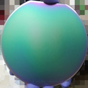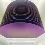
Silicon Epi Wafer

Silicon (Si) epi wafer refers to epitaxially grow one or more layers on a polished wafer substrate by chemical vapor deposition (CVD) or other epitaxial methods. The doping type, resistivity, thickness, lattice structure, etc. of the silicon epitaxial wafer all meet the requirements of specific devices. The silicon epitaxial growth is used to reduce the defects caused by single crystal growth of silicon wafer, so that epi wafer of silicon has a lower defect density and oxygen content, and then is used to manufacture various semiconductor discrete devices and integrated circuit products.
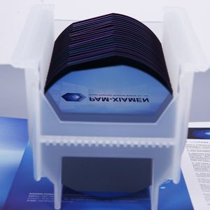
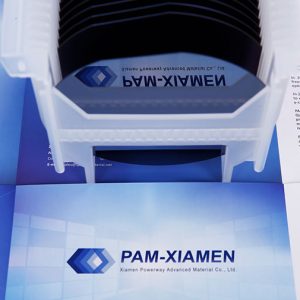
Ganwafer offer Silicon Epitaxial Wafer as follows:
Diameters: 100mm, 125mm, 150mm, 200mm, and 300mm*;
Wafer Orientation: <100>, <111>, <110>;
EPI Thickness: 1µm to 150μm.
We also provide epitaxial customization services.
- Description
- Inquiry
Description
The main technical parameters of epitaxial silicon film include conductivity type, resistivity and uniformity, thickness and uniformity, transition layer thickness, buried epitaxial pattern distortion and pattern drift, surface flatness, dislocation density, surface slippage lines, surface fog, stacking faults and pits, etc. Among them, thickness and resistivity of Si epi wafer are two important inspection items after silicon epitaxial growth.
1. 6″ (150mm) Silicon Epi Wafer Specification
| Item | Specification | |
| Substrate | Sub spec No. | |
| Ingot growth method | CZ | |
| Conductivity type | N | |
| Dopant | As | |
| Orientation | (100)±0.5° | |
| Resistivity | ≤0.005Ohm.cm | |
| RRG | ≤15% | |
| [Oi] Content | 8~18 ppma | |
| Diameter | 150±0.2 mm | |
| Primary Flat Length | 55~60 mm | |
| Primary Flat Location | {110}±1° | |
| Secondly Flat Length | semi | |
| Secondly Flat Location | semi | |
| Thickness | 625±15 um | |
| Backside Characteristics: | ||
| 1. BSD/Poly-Si(A) | 1. BSD | |
| 2. SIO2 | 2. LTO:5000±500 A | |
| 3. Edge Exclusion | 3. EE: 0.6 mm | |
| Laser Marking | NONE | |
| Front surface | Mirror polished | |
| Epi | Structure | N/N+ |
| Dopant | Phos | |
| Thickness | 3±0.2 um | |
| Thk.Uniformity | ≤5 % | |
| Measurement Position | Center(1 pt) 10mm from edge(4 pts @90 degrees) | |
| Calculation | [Tmax-Tmin]÷[[Tmax+Tmin]X100% | |
| Resistivity | 2.5±0.2 Ohm.cm | |
| Res.Uniformity | ≤5 % | |
| Measurement Position | Center(1 pt) 10mm from edge(4 pts @90 degrees) | |
| Calculation | [Rmax-Rmin]÷[[Rmax+Rmin]X100% | |
| Stack fault Density | ≤2 (ea/cm2) | |
| Haze | NONE | |
| Scratches | NONE | |
| Craters, Orange Peel | NONE | |
| Edge Crown | ≤1/3 Epi thickness | |
| Slip(mm) | Total Length ≤ 1Dia | |
| Foreign Matter | NONE | |
| Back Surface Contamination | NONE | |
| Total Point Defects(particle) | ≤30@0.3um |
2. Silicon Epi Process Application
Silicon epi wafers have been successfully used in the manufacture of high-frequency and high-power transistors, and the applications of silicon epitaxy have become more and more extensive. In the bipolar device, whether it is the manufacture of transistors, power tubes, linear integrated circuits and digital integrated circuits, all of these cannot do without silicon epitaxial wafers. For MOS devices, Si epitaxial wafers have been widely used due to the solution of the latch-up effect in CMOS circuits. Currently, BiCMOS circuits are also manufactured using Si epitaxy wafer. Some charge coupled devices (CCD) have been fabricated on epitaxial wafers of silicon.
3. How to Improve the Consistency of Epitaxial Technical Parameters of Silicon Epi Wafer?
The core problem that accompanies mass production is the stability, consistency and uniformity of product parameter control. Only by improving the consistency of silicon wafers in each batch can the quality and yield of epitaxial wafers be improved. Epitaxial wafer manufacturers including us optimize the reaction temperature of the epitaxial layer, the flow rate of the epitaxial gas, the temperature gradient at the center and the edge in the epi wafer process, an epitaxial silicon wafer is achieved with high quality.
For example, according to the characteristics of the silicon epitaxial gas flow field and the CVD reaction mechanism, Si epitaxial growth occurs in the retention layer (substance exchange by diffusion). The higher the position of the reaction interface in the retention layer, the faster the diffusion rate, the higher the corresponding growth rate, and the greater the thickness under the same process time. Therefore, by adjusting the height distribution of the silicon wafer in the airflow field, the epitaxial growth rate on different silicon wafers can be obtained, the adjustment of the epitaxial thickness can be achieved, and a good thickness consistency can be achieved.