LED/LD Epi on Silicon Substrate

Silicon substrates have become one of the substrate materials that global LED/LD suppliers actively invest in research and development. Compared with SiC and sapphire substrates, silicon substrates have two major advantages: firstly, silicon materials are much cheaper than silicon carbide and sapphire, and large-size substrates are easy to obtain, which will significantly reduce the cost of epitaxial growth; secondly, the GaN on Silicon LED lighting epitaxial material is very suitable for stripping the substrate film transfer technology route, and has unique advantages for the development of high-efficiency and high-reliability semiconductor lighting chips.
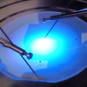
As for the GaN LD, the indirect band gap structure of silicon determines that it is difficult for it to emit light efficiently, while the lasers fabricated on GaN / Si epitaxial wafer have a wide range of applications in information storage, laser display, automotive headlights, visible light communications, submarine communications, and biomedical applications. Growing high-quality GaN-on-Si lasers can not only greatly reduce the manufacturing cost of GaN-based lasers with the help of large-size, low-cost silicon wafers and the automated process lines, but also provide a new technical route for the system integration of lasers and other optoelectronic devices with silicon-based electronic devices.
- Description
- Inquiry
Description
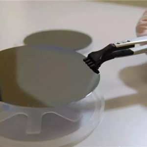
Blue GaN on Si LED wafer and GaN LD Epi on Silicon Substrate can be provided by Ganwafer, a GaN on Si foundry, as follows:
1. Epitaxial Wafer of LED GaN on Silicon with Blue Emission
| LED Epi Parameters | ||||||
| Epi structure: Blue LED | ||||||
| Si(111) substrates ( 1500um) |
t(nm) | Composition | Doping | |||
| A1% | In% | [Si] | [Mg] | |||
| AIN | / | / | / | / | / | |
| AIGaN buffer | / | graded down |
/ | / | / | |
| Undoped GaN | / | / | / | / | ||
| N-GaN | / | / | / | 8.0E+18 | / | |
| MQW ( 7 pairs) |
lnGaN-QW | / | / | 15% | / | / |
| GaN-QB | / | / | / | 2.0E+17 | l | |
| p-AlGaN | / | 15% | / | / | / | |
| P-GaN | / | / | / | / | / | |
| P++ GaN | / | / | / | / | / | |
The chip electrodes of the silicon substrate can be contacted in two ways, namely L contact (Laterial-contact, horizontal contact) and V contact (Vertical-contact), so the current inside the LED chip can flow laterally, or It can flow vertically. Therefore, the current can flow longitudinally; the light-emitting area of the LED is increased, thereby improving the light-emitting efficiency of the LED. GaN on Si epi wafer has become the most potential high-efficiency, low-cost solution for optoelectronics.
In addition, we can offer 2″ InGaN/GaN quantum well blue LD wafer on sapphire or silicon substrate (GANW-190909-GAN-LD):
2. Specification of 440-460nm LD Wafer with GaN on Si Superlattice
| Item | Descriptions | Materials | Substrate |
| blue laser | 440-460nm | InGaN | 2 inch Silicon substrate*** |
| GaN Blue LD EPI Wafer Spec | |||
| Spec | |||
| EPI Wafer Size | |||
| Growth | MOCVD | ||
| Diameter | 50.8 ± 0.2 mm | ||
| Thickness | 430 ± 30 um | ||
| EPI thickness | um | ||
| EPI Wafer Structure | |||
| Contact layer | p type GaN | ||
| Superlattice Cladding Layer | p type GaN | ||
| Electron Blocking Layer | p type AlGaN | ||
| Waveguide Layer | undoped InGaN | ||
| QW and QB layer | InGaN and GaN | ||
| Waveguide Layer | n type InGaN | ||
| Cladding Layer | n type AlGaN | ||
| Substrate | Silicon | ||
Compared with GaN on Si LEDs, the working current density of lasers fabricated on GaN on Si substrate is 2-3 orders of magnitude higher, which requires higher material quality. Moreover, GaN-based end-emitting lasers need to grow a waveguide layer and an optical field confinement layer above and below the quantum well. The optical field confinement layer is usually a low refractive index AlGaN material, which causes additional tensile stress. This makes laser materials grown on GaN on Si epi wafer have much higher requirements than LEDs in terms of stress control and defect control, and the challenges for GaN on Si process are greater.
The performance of our LD GaN on Si epitaxial wafers have reached the international advanced level, and are widely used in 5G communications, laser radar, laser pumping, laser display and other fields.
Remark:
The Chinese government has announced new limits on the exportation of Gallium materials (such as GaAs, GaN, Ga2O3, GaP, InGaAs, and GaSb) and Germanium materials used to make semiconductor chips. From August 1, 2023 on, exporting these materials is only allowed if we obtains a license from the Chinese Ministry of Commerce. Hope for your understanding!