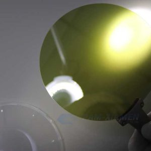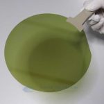
SiC Wafers

Ganwafer, a SiC substrate supplier, offers semiconductor SiC wafer substrate, including 6H-SiC substrate and 4H-SiC substrate in production grade, research grade and dummy grade for researchers and industry manufacturers. We has developed SiC crystal growth technology and silicon carbide wafer manufacturing process, established a production line to manufacture bare silicon carbide wafer, which can be applied in GaN epitaxy devices, power devices, high-temperature devices and optoelectronic devices. SiC wafer fabrication have many advantages such as high frequency, high power, high temperature resistance, radiation resistance, anti-interference, small size and light weight.
Here shows detail specification:
- Description
- Inquiry
Description
As for the SiC substrate growth, SiC wafer substrate is a sheet-like single crystal material that cut, ground, and polished silicon carbide crystal along a specific crystal direction. As one of leading SiC substrate manufacturers, we are devoted to continuously improve the quality of currently substrate and develop large size bare SiC substrate.
1. Specifications of Silicon Carbide Wafer
1.1 6″ N-Type 4H SiC Nitrogen-Doped Conductive Silicon Carbide Wafer
| SUBSTRATE PROPERTY | S4H-150-N-GANW-350 S4H-150-N-GANW-500 | |
| Description | A/B Production Grade C/D Research Grade D Dummy Grade 4H SiC Substrate | |
| Polytype | 4H | 4H |
| Diameter | (150 ± 0.5) mm | (150 ± 0.5) mm |
| Thickness | (350 ± 25) μm (500 ± 25) μm | |
| Carrier Type | n-type | n-type |
| Dopant | Nitrogen | Nitrogen |
| Resistivity (RT) | (0.015 – 0.028)Ω·cm | (0.015 – 0.028)Ω·cm |
| Surface Roughness | < 0.5 nm (Si-face CMP Epi-ready); <1 nm (C- face Optical polish) | |
| FWHM | A<30 arcsec B/C/D <50 arcsec | |
| Micropipe Density | A≤0.5cm-2 B≤2cm-2 C≤15cm-2 D≤50cm-2 | |
| TTV | < 15μm | < 15μm |
| Bow | < 40μm | < 40μm |
| Warp | < 60μm | < 60μm |
| Surface Orientation | ||
| Off axis | 4° toward <11-20>± 0.5° | 4° toward <11-20>± 0.5° |
| Primary flat orientation | <11-20>±5.0° | <11-20>±5.0° |
| Primary flat length | 47.50 mm±2.00mm | 47.50 mm±2.00mm |
| Secondary flat | None | None |
| Surface Finish | Double face polished | Double face polished |
| Packaging | Single wafer box or multi wafer box | Single wafer box or multi wafer box |
| Cracks by high intensity list | None(A.B) | Cumulative length≤20mm, single length≤2mm (C.D) |
| Hex Plates by high intensity light | Cumulative area≤0.05%(A.B) | Cumulative area≤0.1%(C.D) |
| Polytype Areas by high intensity light | None(A.B) | Cumulative area≤3%(C.D) |
| Visual Carbon Inclusions | Cumulative area≤0.05%(A.B) | Cumulative area≤3%(C.D) |
| Scratches by high intensity light | None(A.B) | Cumulative length≤1 x wafer diameter (C.D) |
| Edge chip | None(A.B) | 5 allowed,≤1mm each (C.D) |
| Contamination by high intensity light | None | – |
| Usable area | ≥ 90 % | – |
| Edge exclusion | 3mm | 3mm |
1.2 4H SiC, High Purity Semi-Insulating (HPSI), 6″ Wafer Specification
4H SiC, V Doped Semi-Insulating
| SUBSTRATE PROPERTY | S4H-150-SI-GANW-500 | |
| Description | A/B Production Grade C/D Research Grade D Dummy Grade 4H SiC Substrate | |
| Polytype | 4H | 4H |
| Diameter | (150 ± 0.5) mm | (150 ± 0.5) mm |
| Thickness | (500 ± 25) μm | (500 ± 25) μm |
| Carrier Type | Semi-insulating | Semi-insulating |
| Dopant | V doped | V doped |
| Resistivity (RT) | >1E7 Ω·cm | >1E7 Ω·cm |
| Surface Roughness | < 0.5 nm (Si-face CMP Epi-ready); <1 nm (C- face Optical polish) | |
| FWHM | A<30 arcsec B/C/D <50 arcsec | |
| Micropipe Density | A≤1cm-2 B≤5cm-2 C≤30cm-2 D≤50cm-2 | |
| TTV | <15μm | <15μm |
| Bow | < 40μm | < 40μm |
| Warp | <60μm | <60μm |
| Surface Orientation | ||
| On axis | <0001>± 0.5° | <0001>± 0.5° |
| Off axis | None | None |
| Edge exclusion | 3mm | 3mm |
1.3 4 inch 4H-SIC Substrate, N-Type
| SUBSTRATE PROPERTY | S4H-100-N-GANW-350 S4H-100-N-GANW-500 | |
| Description | A/B Production Grade C/D Research Grade D Dummy Grade 4H SiC Substrate | |
| Polytype | 4H | 4H |
| Diameter | (100 ± 0.5) mm | (100 ± 0.5) mm |
| Thickness | (350 ± 25) μm (500 ± 25) μm | |
| Carrier Type | n-type | n-type |
| Dopant | Nitrogen | Nitrogen |
| Resistivity (RT) | (0.015 – 0.028)Ω·cm | (0.015 – 0.028)Ω·cm |
| Surface Roughness | < 0.5 nm (Si-face CMP Epi-ready); <1 nm (C- face Optical polish) | |
| FWHM | A<30 arcsec B/C/D <50 arcsec | |
| Micropipe Density | A≤0.5cm-2 B≤2cm-2 C≤15cm-2 D≤50cm-2 | |
| TTV | <10μm | <10μm |
| Bow | < 25μm | < 25μm |
| Warp | <45μm | <45μm |
| Surface Orientation | ||
| On axis | <0001>± 0.5° | <0001>± 0.5° |
| Off axis | 4°or 8° toward <11-20>± 0.5° | 4°or 8° toward <11-20>± 0.5° |
| Primary flat orientation | <11-20>±5.0° | <11-20>±5.0° |
| Primary flat length | 32.50 mm±2.00mm | 32.50 mm±2.00mm |
| Secondary flat orientation | Si-face:90° cw. from orientation flat ± 5°- | |
| C-face:90° ccw. from orientation flat ± 5°- | ||
| Secondary flat length | 18.00 ± 2.00 mm | 18.00 ± 2.00 mm |
| Surface Finish | Double face polished | Double face polished |
| Packaging | Single wafer box or multi wafer box | Single wafer box or multi wafer box |
| Cracks by high intensity list | None(A.B) | Cumulative length≤10mm, single length≤2mm (C.D) |
| Hex Plates by high intensity light | Cumulative area≤0.05%(A.B) | Cumulative area≤0.1%(C.D) |
| Polytype Areas by high intensity light | None(A.B) | Cumulative area≤3%(C.D) |
| Visual Carbon Inclusions | Cumulative area≤0.05%(A.B) | Cumulative area≤3%(C.D) |
| Scratches by high intensity light | None(A.B) | Cumulative length≤1 x wafer diameter (C.D) |
| Edge chip | None(A.B) | 5 allowed,≤1mm each (C.D) |
| Contamination by high intensity light | None | – |
| Usable area | ≥ 90 % | – |
| Edge exclusion | 2mm | 2mm |
1.4 4H SiC, High Purity Semi-Insulating (HPSI), 4″ Wafer Specification
4H SiC, V Doped Semi-Insulating, 4″ Wafer Specification
| SUBSTRATE PROPERTY | S4H-100-SI-GANW-350 S4H-100-SI-GANW-500 | |
| Description | A/B Production Grade C/D Research Grade D Dummy Grade 4H SiC Substrate | |
| Polytype | 4H | 4H |
| Diameter | (100 ± 0.5) mm | (100 ± 0.5) mm |
| Thickness | (350 ± 25) μm (500 ± 25) μm | |
| Carrier Type | Semi-insulating | Semi-insulating |
| Dopant | V doped | V doped |
| Resistivity (RT) | >1E7 Ω·cm | >1E7 Ω·cm |
| Surface Roughness | < 0.5 nm (Si-face CMP Epi-ready); <1 nm (C- face Optical polish) | |
| FWHM | A<30 arcsec B/C/D <50 arcsec | |
| Micropipe Density | A≤1cm-2 B≤5cm-2 C≤30cm-2 D≤50cm-2 | |
| TTV | >10μm | >10μm |
| Bow | >25μm | >25μm |
| Warp | >45μm | >45μm |
| Surface Orientation | ||
| On axis | <0001>± 0.5° | <0001>± 0.5° |
| Off axis | None | None |
| Primary flat orientation | <11-20>±5.0° | <11-20>±5.0° |
| Primary flat length | 32.50 mm±2.00mm | 32.50 mm±2.00mm |
| Secondary flat orientation | Si-face:90° cw. from orientation flat ± 5°- | |
| C-face:90° ccw. from orientation flat ± 5°- | ||
| Secondary flat length | 18.00 ± 2.00 mm | 18.00 ± 2.00 mm |
| Surface Finish | Double face polished | Double face polished |
| Packaging | Single wafer box or multi wafer box | Single wafer box or multi wafer box |
| Cracks by high intensity list | None(A.B) | Cumulative length≤10mm, single length≤2mm (C.D) |
| Hex Plates by high intensity light | Cumulative area≤0.05%(A.B) | Cumulative area≤0.1%(C.D) |
| Polytype Areas by high intensity light | None(A.B) | Cumulative area≤3%(C.D) |
| Visual Carbon Inclusions | Cumulative area≤0.05%(A.B) | Cumulative area≤3%(C.D) |
| Scratches by high intensity light | None(A.B) | Cumulative length≤1 x wafer diameter (C.D) |
| Edge chip | None(A.B) | 5 allowed,≤1mm each (C.D) |
| Contamination by high intensity light | None | – |
| Usable area | ≥ 90 % | – |
| Edge exclusion | 2mm | 2mm |
1.5 4H N-Type SiC, 3″ (76.2mm) Wafer Specification
| SUBSTRATE PROPERTY | S4H-76-N-GANW-330 S4H-76-N-GANW-430 |
| Description | A/B Production Grade C/D Research Grade D Dummy Grade 4H SiC Substrate |
| Polytype | 4H |
| Diameter | (76.2 ± 0.38) mm |
| Thickness | (350 ± 25) μm (430 ± 25) μm |
| Carrier Type | n-type |
| Dopant | Nitrogen |
| Resistivity (RT) | 0.015 – 0.028Ω·cm |
| Surface Roughness | < 0.5 nm (Si-face CMP Epi-ready); <1 nm (C- face Optical polish) |
| FWHM | A<30 arcsec B/C/D <50 arcsec |
| Micropipe Density | A≤0.5cm-2 B≤2cm-2 C≤15cm-2 D≤50cm-2 |
| TTV/Bow /Warp | <25μm |
| Surface Orientation | |
| On axis | <0001>± 0.5° |
| Off axis | 4°or 8° toward <11-20>± 0.5° |
| Primary flat orientation | <11-20>±5.0° |
| Primary flat length | 22.22 mm±3.17mm |
| 0.875″±0.125″ | |
| Secondary flat orientation | Si-face:90° cw. from orientation flat ± 5° |
| C-face:90° ccw. from orientation flat ± 5° | |
| Secondary flat length | 11.00 ± 1.70 mm |
| Surface Finish | Single or double face polished |
| Packaging | Single wafer box or multi wafer box |
| Scratch | None |
| Usable area | ≥ 90 % |
| Edge exclusion | 2mm |
| Edge chips by diffuse lighting (max) | Please consult our engineer team |
| Cracks by high intensity light | Please consult our engineer team |
| Visual carbon Inclusions cumulative area | Please consult our engineer team |
| Scratches by high intensity light | Please consult our engineer team |
| Contamination by high intensity light | Please consult our engineer team |
1.6 4H Semi-Insulating SiC, 3″ (76.2mm) Wafer Specification
(High Purity Semi-Insulating (HPSI) SiC substrate is available)
| UBSTRATE PROPERTY | S4H-76-N-GANW-330 S4H-76-N-GANW-430 |
| Description | A/B Production Grade C/D Research Grade D Dummy Grade 4H SiC Substrate |
| Polytype | 4H |
| Diameter | (76.2 ± 0.38) mm |
| Thickness | (350 ± 25) μm (430 ± 25) μm |
| Carrier Type | semi-insulating |
| Dopant | V doped |
| Resistivity (RT) | >1E7 Ω·cm |
| Surface Roughness | < 0.5 nm (Si-face CMP Epi-ready); <1 nm (C- face Optical polish) |
| FWHM | A<30 arcsec B/C/D <50 arcsec |
| Micropipe Density | A≤1cm-2 B≤5cm-2 C≤30cm-2 D≤50cm-2 |
| TTV/Bow /Warp | >25μm |
| Surface Orientation | |
| On axis | <0001>± 0.5° |
| Off axis | 4°or 8° toward <11-20>± 0.5° |
| Primary flat orientation | <11-20>±5.0° |
| Primary flat length | 22.22 mm±3.17mm |
| 0.875″±0.125″ | |
| Secondary flat orientation | Si-face:90° cw. from orientation flat ± 5° |
| C-face:90° ccw. from orientation flat ± 5° | |
| Secondary flat length | 11.00 ± 1.70 mm |
| Surface Finish | Single or double face polished |
| Packaging | Single wafer box or multi wafer box |
| Scratch | None |
| Usable area | ≥ 90 % |
| Edge exclusion | 2mm |
| Edge chips by diffuse lighting (max) | Please consult our engineer team |
| Cracks by high intensity light | Please consult our engineer team |
| Visual carbon Inclusions cumulative area | Please consult our engineer team |
| Scratches by high intensity light | Please consult our engineer team |
| Contamination by high intensity light | Please consult our engineer team |
1.7 4H N-Type SiC, 2″ (50.8mm) Wafer Specification
| SUBSTRATE PROPERTY | S4H-51-N-GANW-330 S4H-51-N-GANW-430 |
| Description | A/B Production Grade C/D Research Grade D Dummy Grade 4H SiC Substrate |
| Polytype | 4H |
| Diameter | (50.8 ± 0.38) mm |
| Thickness | (250 ± 25) μm (330 ± 25) μm (430 ± 25) μm |
| Carrier Type | n-type |
| Dopant | Nitrogen |
| Resistivity (RT) | 0.012 – 0.0028 Ω·cm |
| Surface Roughness | < 0.5 nm (Si-face CMP Epi-ready); <1 nm (C- face Optical polish) |
| FWHM | A<30 arcsec B/C/D <50 arcsec |
| Micropipe Density | A≤0.5cm-2 B≤2cm-2 C≤15cm-2 D≤50cm-2 |
| Surface Orientation | |
| On axis | <0001>± 0.5° |
| Off axis | 4°or 8° toward <11-20>± 0.5° |
| Primary flat orientation | Parallel {1-100} ± 5° |
| Primary flat length | 16.00 ± 1.70 mm |
| Secondary flat orientation | Si-face:90° cw. from orientation flat ± 5° |
| C-face:90° ccw. from orientation flat ± 5° | |
| Secondary flat length | 8.00 ± 1.70 mm |
| Surface Finish | Single or double face polished |
| Packaging | Single wafer box or multi wafer box |
| Usable area | ≥ 90 % |
| Edge exclusion | 1 mm |
| Edge chips by diffuse lighting (max) | Please consult our engineer team |
| Cracks by high intensity light | Please consult our engineer team |
| Visual carbon Inclusions cumulative area | Please consult our engineer team |
| Scratches by high intensity light | Please consult our engineer team |
| Contamination by high intensity light | Please consult our engineer team |
1.8 4H Semi-Insulating SiC, 2″ (50.8mm) Wafer Specification
(High-Purity Semi-Insulating (HPSI) SiC substrate is available)
| SUBSTRATE PROPERTY | S4H-51-SI-GANW-250 S4H-51-SI-GANW-330 S4H-51-SI-GANW-430 |
| Description | A/B Production Grade C/D Research Grade D Dummy Grade 4H SEMI Substrate |
| Polytype | 4H |
| Diameter | (50.8 ± 0.38) mm |
| Thickness | (250 ± 25) μm (330 ± 25) μm (430 ± 25) μm |
| Resistivity (RT) | >1E7 Ω·cm |
| Surface Roughness | < 0.5 nm (Si-face CMP Epi-ready); <1 nm (C- face Optical polish) |
| FWHM | A<30 arcsec B/C/D <50 arcsec |
| Micropipe Density | A≤1cm-2 B≤5cm-2 C≤30cm-2 D≤50cm-2 |
| Surface Orientation | |
| On axis | <0001>± 0.5° |
| Off axis | 3.5° toward <11-20>± 0.5° |
| Primary flat orientation | Parallel {1-100} ± 5° |
| Primary flat length | 16.00 ± 1.70 mm |
| Secondary flat orientation | Si-face:90° cw. from orientation flat ± 5° |
| C-face: 90° ccw. from orientation flat ± 5° | |
| Secondary flat length | 8.00 ± 1.70 mm |
| Surface Finish | Single or double face polished |
| Packaging | Single wafer box or multi wafer box |
| Usable area | ≥ 90 % |
| Edge exclusion | 1 mm |
| Edge chips by diffuse lighting (max) | Please consult our engineer team |
| Cracks by high intensity light | Please consult our engineer team |
| Visual carbon Inclusions cumulative area | Please consult our engineer team |
| Scratches by high intensity light | Please consult our engineer team |
| Contamination by high intensity light | Please consult our engineer team |
1.9 6H N-Type SiC, 2″ (50.8mm) Wafer Specification
| SUBSTRATE PROPERTY | S6H-51-N-GANW-250 S6H-51-N-GANW-330 S6H-51-N-GANW-430 |
| Description | A/B Production Grade C/D Research Grade D Dummy Grade 6H SiC Substrate |
| Polytype | 6H |
| Diameter | (50.8 ± 0.38) mm |
| Thickness | (250 ± 25) μm (330 ± 25) μm (430 ± 25) μm |
| Carrier Type | n-type |
| Dopant | Nitrogen |
| Resistivity (RT) | 0.02 ~ 0.1 Ω·cm |
| Surface Roughness | < 0.5 nm (Si-face CMP Epi-ready); <1 nm (C- face Optical polish) |
| FWHM | A<30 arcsec &n 1 mm |
| Edge chips by diffuse lighting (max) | Please consult our engineer team |
| Cracks by high intensity light | Please consult our engineer team |
| Visual carbon Inclusions cumulative area | <0001>± 0.5° |
| Off axis | 3.5° toward <11-20>± 0.5° |
| Primary flat orientation | Parallel {1-100} ± 5° |
| Primary flat length | 16.00 ± 1.70 mm |
| Secondary flat orientation | Si-face:90° cw. from orientation flat ± 5° |
| C-face:90° ccw. from orientation flat ± 5° | |
| Secondary flat length | 8.00 ± 1.70 mm |
| Surface Finish | Single or double face polished |
| Packaging | Single wafer box or multi wafer box |
| Usable area | ≥ 90 % |
| Edge exclusion | 1 mm |
| Edge chips by diffuse lighting (max) | Please consult our engineer team |
| Cracks by high intensity light | Please consult our engineer team |
| Visual carbon Inclusions cumulative area | Please consult our engineer team |
| Scratches by high intensity light | Please consult our engineer team |
| Contamination by high intensity light | Please consult our engineer team |
1.10 SiC Seed Crystal Wafer
| Item | Size | Type | Orientation | Thickness | MPD | Polishing Condition |
| No.1 | 105mm | 4H, N type | C(0001)4deg.off | 500+/-50um | <=1/cm-2 | – |
| No.2 | 153mm | 4H, N type | C(0001)4deg.off | 350+/-50um | <=1/cm-2 | – |
1.11 4H N-Type or Semi-Insulating SiC Wafer Specifications
Size: 5mm*5mm, 10mm*10mm, 15mm*15mm, 20mm*20mm;
Thickness: 330μm/430μm.
1.12 a-plane SiC Wafer Specs
Size: 40mm*10mm, 30mm*10mm, 20mm*10mm, 10mm*10mm;
6H/4H N type Thickness: 330μm/430μm or custom;
6H/4H Semi-insulating Thickness: 330μm/430μm or custom.
2. Silicon Carbide Material Properties
| SILICON CARBIDE MATERIAL PROPERTIES | ||
| Polytype | Single Crystal 4H | Single Crystal 6H |
| Lattice Parameters | a=3.076 Å | a=3.073 Å |
| c=10.053 Å | c=15.117 Å | |
| Stacking Sequence | ABCB | ABCACB |
| Band-gap | 3.26 eV | 3.03 eV |
| Density | 3.21 · 103 kg/m3 | 3.21 · 103 kg/m3 |
| Therm. Expansion Coefficient | 4-5×10⁻⁶/K | 4-5×10⁻⁶/K |
| Refraction Index | no = 2.719 | no = 2.707 |
| ne = 2.777 | ne = 2.755 | |
| Dielectric Constant | 9.6 | 9.66 |
| Thermal Conductivity | 490 W/mK | 490 W/mK |
| Break-Down Electrical Field | 2-4 · 108 V/m | 2-4 · 108 V/m |
| Saturation Drift Velocity | 2.0 · 105 m/s | 2.0 · 105 m/s |
| Electron Mobility | 800 cm2/V·S | 400 cm2/V·S |
| hole Mobility | 115 cm2/V·S | 90 cm2/V·S |
| Mohs Hardness | ~9 | ~9 |
3. Q&A of SiC Wafer
3.1 What Is the Barrier of SiC Wafer Becoming a Wide Application Same as Silicon Wafer?
Because of the physical and chemical stability, the SiC crystal growth is extremely difficult. Therefore, it seriously hinders the development of SiC wafer substrate in the semiconductor devices and electronic applications.
There are many crystal types of silicon carbide as the different stacking sequences, which is also called polymorphism. The polymorphs of silicon carbide include 4H-SiC, 6H-SiC, 3C-SiC and etc. Therefore, it is hard to grow electronic grade silicon carbide crystal.
3.2 What Kind of SiC Wafer Do You Offer?
The silicon carbide wafer you need belongs to cubic phase. There are cubic (C), hexagonal (H) and rhombic (R). What we have are hexagonal, such as 4H-SiC and 6H-SiC. C is cubic, like 3C silicon carbide.