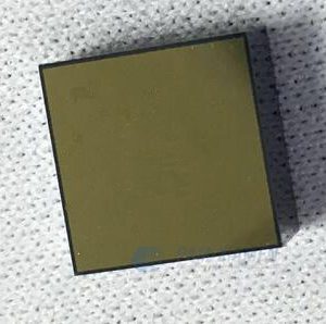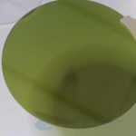
Germanium Wafer
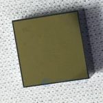
Single crystal Ge (Germanium) wafers grown by VGF / LEC can be offered by a germanium wafer manufacturer – Ganwafer.
Semiconductor devices fabricated on Ge wafer are used as diodes, transistors and composite transistors, and semiconductor optoelectronic devices on Germanium are used as photoelectric, Hall and piezoresistive sensors, photoconductive effect radiation detectors, etc. Most of the applications of Ge based semiconductor devices have been replaced by silicon. There is a certain amount of Ge crystal wafer used in high-frequency and high-power devices, while a large amount in photoelectric avalanche diodes.
Use single crystal Ge wafer to make a GaAs/Ge solar cell. The performance of Ge-based solar cell is close to that of a GaAs/GaAs cell, with higher mechanical strength and a larger monolithic cell area. In the space application environment, the anti-radiation threshold is higher than that of silicon cells, the performance degradation is small, and its application cost is close to the same power of silicon cell panels. Solar cell fabricated on bulk Ge substrate has been used in various types of military satellites and some commercial satellites, and has gradually become the main space power source. More about Ge single crystal wafer please see below:
- Description
- Inquiry
Description
1. General Properties of Ge Wafer
| General Properties Structure | Cubic, a = 5.6754 Å | ||
| Density: 5.765 g/cm3 | |||
| Melting Point: 937.4 °C | |||
| Thermal Conductivity: 640 | |||
| Crystal Growth Technology | Czochralski | ||
| Doping available | / | Sb Doping | Doping In or Ga |
| Conductive Type | N | N | P |
| Resistivity, ohm.cm | >35 | < 0.05 | 0.05 – 0.1 |
| EPD | < 5×10^3/cm2 | < 5×10^3/cm2 | < 5×10^3/cm2 |
| < 5×10^2/cm2 | < 5×10^2/cm2 | < 5×10^2/cm2 | |
2. Grades and Application of Bulk Ge Substrate
| Electronic Grade | Used for diodes and transistors, |
| Infrared or opitical Grade | Used for IR optical window or disks, optical components |
| Cell Grade | Used for substrates of solar cell |
3. Standard Specs of Ge Crystal and Wafer
| Crystal Orientation | <111>,<100> and <110> ± 0.5° or custom orientation | |||
| Crystal boule as grown | 1″ ~ 6″ diameter x 200 mm Length | |||
| Standard blank as cut | 1″x 0.5mm | 2″x0.6mm | 4″x0.7mm | 5″&6″x0.8mm |
| Standard Polished wafer(One/two sides polished) | 1″x 0.30 mm | 2″x0.5mm | 4″x0.5mm | 5″&6″x0.6mm |
4. Special size and orientation are available upon requested germanium wafer:
4.1 Specification of Single Crystal Germanium Wafer
| Item | Specifications | Remarks |
| Growth Method | VGF | |
| Conduction Type | n-type, p type | |
| Dopant | Gallium or Antimony | |
| Wafer Diameter | 2, 3, 4 & 6 | inch |
| Crystal Orientation | (100), (111), (110) | |
| Thickness | 200~550 | um |
| OF | EJ or US | |
| Carrier Concentration | request upon customers | |
| Resistivity at RT | (0.001~80) | Ohm.cm |
| Etch Pit Density | <5000 | /cm2 |
| Laser Marking | upon request | |
| Surface Finish | P/E or P/P | |
| Epi ready | Yes | |
| Package | Single wafer container or cassette |
4.2 Specification of Single Crystal Ge Wafer
| 4 inch Ge wafer Specification | for Solar Cells | |
| Doping | P | |
| Doping substances | Ge-Ga | |
| Diameter | 100±0.25 mm | |
| Orientation | (100) 9° off toward <111>+/-0.5° | |
| Off-orientation tilt angle | N/A | |
| Primary Flat Orientation | N/A | |
| Primary Flat Length | 32±1 | mm |
| Secondary Flat Orientation | N/A | |
| Secondary Flat Length | N/A | mm |
| cc | (0.26-2.24)E18 | /c.c |
| Resistivity | (0.74-2.81)E-2 | ohm.cm |
| Electron Mobility | 382-865 | cm2/v.s. |
| EPD | <300 | /cm2 |
| Laser Mark | N/A | |
| Thickness | 175±10 | μm |
| TTV | <15 | μm |
| TIR | N/A | μm |
| BOW | <10 | μm |
| Warp | <10 | μm |
| Front face | Polished | |
| Back face | Ground | |
5. Germanium Wafer Process
In the electronics grade and IR grade Ge wafer production process, germanium dioxide from the residue processing is further purified in chlorination and hydrolysis steps.
1) High purity germanium is obtained during zone refining;
2) A Ge crystal is produced via the Czochralski process;
3) The Ge wafer is manufactured via several cutting, grinding, and etching steps;
4) The wafers are cleaned and inspection. During this process, the wafers are single side polished or double side polished according to custom requirement, epi-ready wafer comes;
5) The wafers are packed in single wafer containers, under a nitrogen atmosphere.
6. Germanium Applications
Germanium blank or window is used in night vision and thermographic imaging solutions for commercial security, firefighting and industrial monitoring equipment. Also, they are used as filters for analytical and measuring equipment, windows for remote temperature measurement, and mirrors for lasers.
Thin Ge single crystal wafers are used in III-V triple-junction solar cells and for power Concentrated PV (CPV) systems.
Remark:
The Chinese government has announced new limits on the exportation of Gallium materials (such as GaAs, GaN, Ga2O3, GaP, InGaAs, and GaSb) and Germanium materials used to make semiconductor chips. From August 1, 2023 on, exporting these materials is only allowed if we obtains a license from the Chinese Ministry of Commerce. Hope for your understanding!