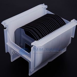
The semiconductor chip manufacturing process can be roughly divided into several steps, such as wafer fabrication, wafer probe, packaging, and initial test and final test. Among them, the semiconductor wafer fabrication steps and the wafer probe test process are the front end semiconductor wafer manufacturing process, and the assembly process and the test process are the back end semiconductor manufacturing process.
The main work of wafer manufacturing process from fab of Ganwafer is to make circuits and electronic components (such as transistors, capacitors, logic switches, etc.) on the wafer. The semiconductor manufacturing process steps are usually related to the product type and the semiconductor manufacturing technology used. Generally, the basic steps are to clean the wafer properly, then perform oxidation and chemical vapor deposition on its surface, and then perform repeated wafer making process such as coating, exposure, development, etching, ion implantation, and metal sputtering. Finally, several layers of circuits and components are processed and fabricated on the wafer.
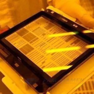
Wafer probe test process is after the previous process. A small grid, that is, dies, is formed on the wafer. Generally, in order to facilitate testing and improve efficiency, the same type of wafer is produced on the same wafer. However, several products of different varieties and specifications can also be produced according to needs, and then each crystal grain can be inspected with a probe instrument.
As a highly experienced and skilled semiconductor wafer manufacturing company, we perform all these steps precisely to meet client’s expectations and demands. We produce and supply industry-standard products within budget.