Who Are Ganwafer?
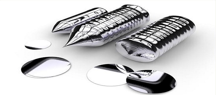
கன்வேஃபர் என்பது செமிகண்டக்டர் படிக வளர்ச்சி, செயல்முறை மேம்பாடு மற்றும் எபிடாக்ஸியை ஒருங்கிணைக்கும் கலவை குறைக்கடத்தி பொருளுக்கான ஒரு உயர்தர நிறுவனமாகும். SiC&GaN மெட்டீரியல் (SiC வேஃபர் மற்றும் எபிடாக்ஸி, GaN வேஃபர் மற்றும் எபி வேஃபர்) மற்றும் III-V மெட்டீரியல் (III-V அடி மூலக்கூறு மற்றும் எபி சேவை: InP வேஃபர், GaSb வேஃபர், GaAs வேஃபர், போன்ற கலவை குறைக்கடத்தி செதில்களின் ஆராய்ச்சி மற்றும் உற்பத்தியில் நாங்கள் நிபுணத்துவம் பெற்றுள்ளோம். InAs wafer, and InSb wafer).
ஒரு முன்னணி ஆராய்ச்சி மற்றும் உற்பத்தி நிறுவனமாக, 1990 முதல் CZ சிலிக்கான் வேஃபர் மற்றும் இங்காட்களை ஆராய்ச்சி செய்து உருவாக்குவதற்கும் > 1000 ohm.cm உடன் FZ சிலிக்கான் செதில்களை உருவாக்குவதற்கும் நாங்கள் அர்ப்பணித்துள்ளோம். பிரைம் கிரேடு மற்றும் டெஸ்ட் கிரேடு மூலம் 2” முதல் 12” வரையிலான செதில் அளவுகளை எங்களால் வழங்க முடியும்.
Semiconductor wafers from Ganwafer are used in various applications. They are hugely used in LED semiconductor lighting, wireless communication, solar power, infrared device, laser, detectors, and semiconductor power devices, including power devices, high-temperature devices, and photoelectric devices, therein, GaN wafer including GaN on Si, GaN on SiC, and GaN on Sapphire are for Mini/micro LED, power electronics and microwave RF.
Why Ganwafer?
எமது பலம்
எங்களிடம் ஒரு வலுவான தொழில்நுட்ப R & D குழுவின் நிபுணர் குழு உள்ளது, இது பிரபல தலைமை விஞ்ஞானிகளால் வழிநடத்தப்படுகிறது, மேலும் வலுவான R & D வலிமையைக் கொண்டுள்ளது. எதிர்பார்க்கப்படும் தயாரிப்புகளை திறம்பட உற்பத்தி செய்வதற்கான சிறந்த வேஃபர் ஃபவுண்டரி எங்களிடம் உள்ளது. புதிய தயாரிப்பு வகைகளை உருவாக்க உதவும் சந்தைப் போக்கின்படி சமீபத்திய பொருள் மற்றும் சாதனங்களைப் பற்றிய சிறந்த புரிதலை எங்கள் நிபுணர்கள் பெற்றுள்ளனர். தற்போதுள்ள தயாரிப்பின் தரத்தை தொடர்ந்து மேம்படுத்துவதை நோக்கமாகக் கொண்டுள்ளோம்.
தரமான தயாரிப்பு
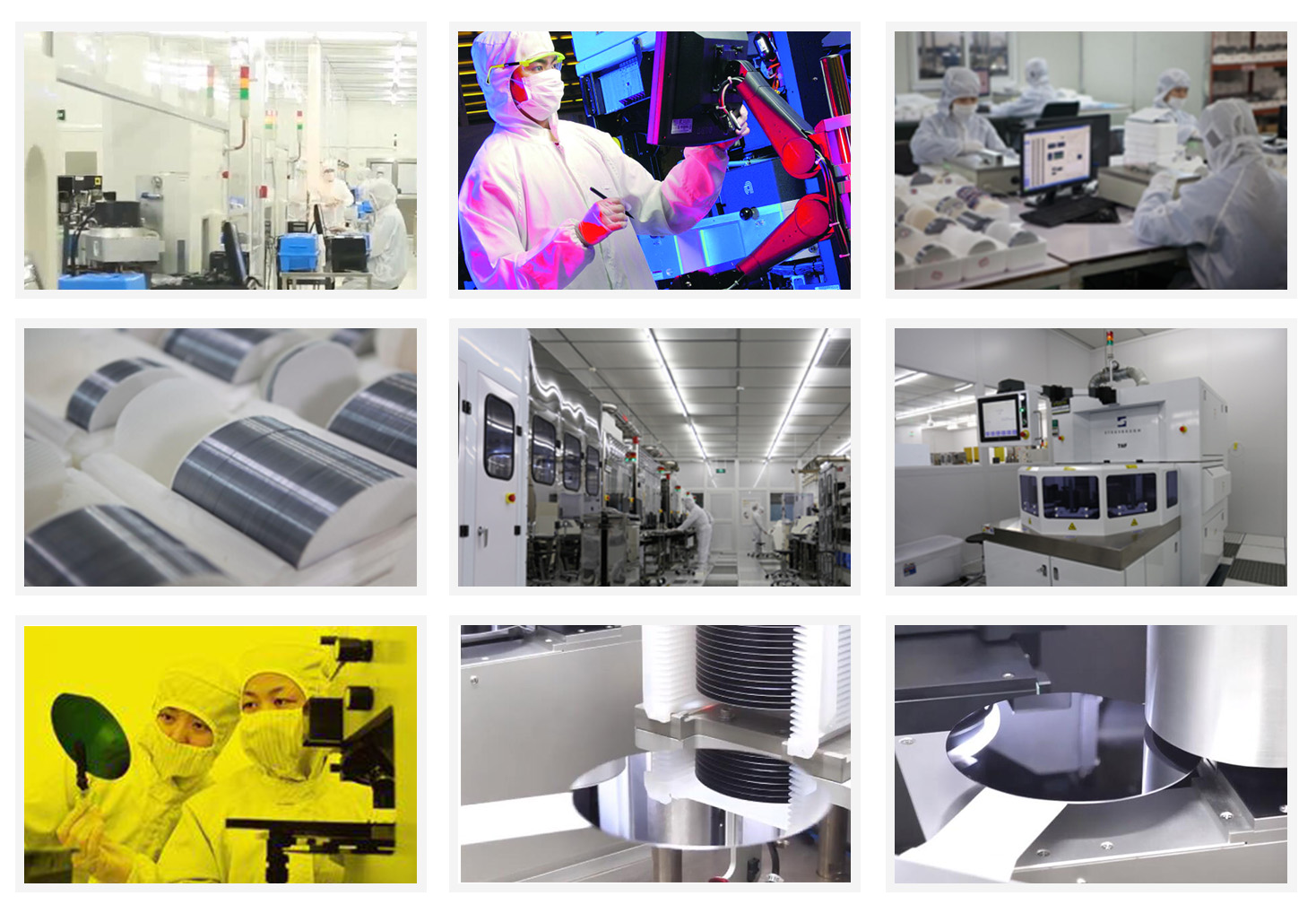
Ganwafer has been ISO9001:2015, owns and shares four modern foundries that able to deliver a range of industry-standard products with utmost quality. We ensure that our produced advanced wafer will meet clients’ needs, specifications, and budgets. We have been operating in this industry for many years that makes us stand out from the market. Each process of wafer manufacturing will be handled through our severe quality system. You can expect test reports for each shipment and each wafer are warranty.
25+ வருட அனுபவங்கள்
பொருள் தயாரித்தல் மற்றும் அதனுடன் தொடர்புடைய உபகரண வடிவமைப்பு மற்றும் மேம்பாடு மற்றும் பொருட்களின் இயற்பியல், இரசாயன மற்றும் மின் பண்புகள், பொருள் தயாரிக்கும் செயல்முறை பற்றிய கடினமான ஆராய்ச்சி ஆகியவற்றில் எங்களுக்கு ஏராளமான அனுபவம் உள்ளது. விஞ்ஞான மற்றும் தொழில்நுட்ப பணியாளர்களின் தத்துவார்த்த படிவு மற்றும் நடைமுறை அனுபவம் பற்றிய பரந்த அறிவு எங்கள் நிறுவனத்தின் முக்கிய சக்தியாகும்.
தொடர்புடைய பொருட்கள் மற்றும் உபகரணங்களின் விரிவாக்கத்தில் நிபுணத்துவம் பெற்ற ஆண்டுகள் சிறந்த தயாரிப்பு தரம் மற்றும் செயல்திறனுக்கு உத்தரவாதம் அளிக்கிறது. எங்கள் உபகரண வடிவமைப்பு திட்டம் பயனர்களின் உண்மையான தொழில்நுட்ப மற்றும் தொழில்நுட்ப தேவைகளை பூர்த்தி செய்ய முடியும். பொருட்கள் மேம்பாட்டின் எங்களின் வளமான வரலாறு, எங்கள் நிறுவனத்தை சந்தையில் இருந்து தனித்து நிற்கச் செய்து, இந்தத் துறையில் பல்வேறு வகையான கலவை செமிகண்டக்டர் வகைகளில் தொழில்துறையில் முன்னணி அதிகாரியாக ஒரு அளவுகோலை அமைக்கிறது.
உயர்ந்த தரம்
தரத்தில் சமரசம் செய்யாமல் தொழில்துறை தரத்தின்படி உயர்தர தயாரிப்புகளை வழங்குவது எங்கள் முதன்மையான முன்னுரிமையாகும். சிறந்த வாடிக்கையாளர் சேவையை நாங்கள் உறுதி செய்கிறோம். எங்கள் விற்பனைப் பிரதிநிதிகள் உங்கள் வினவல்களை அழிப்பார்கள் மற்றும் விநியோகஸ்தர்கள் மென்மையான சுங்கம் மற்றும் கப்பல் நடைமுறைகளை உறுதி செய்வார்கள். எங்கள் மதிப்பிற்குரிய வாடிக்கையாளர்கள் தங்கள் தயாரிப்புகளை எந்த தொந்தரவும் இல்லாமல் எளிதாக வாங்க முடியும். வாடிக்கையாளர்கள் தங்கள் பட்ஜெட் வரம்பிற்குள் மலிவு விலையில் ஒப்பந்தத்தைப் பெறுவார்கள் மற்றும் அவர்களின் பணத்திற்கான சிறந்த மதிப்பைப் பெறுவார்கள்.
நல்ல விற்பனை சேவை
வெவ்வேறு வாடிக்கையாளர்களுடன் தேவைகள் மற்றும் விவரக்குறிப்புகள் மாறுபடும் மற்றும் திட்ட அளவும் மாறுபடும் என்பதை நாங்கள் புரிந்துகொள்கிறோம். கவலைப்படவே வேண்டாம்! உங்களுக்கு உதவ நாங்கள் இருக்கிறோம். உங்களின் அனைத்து தேவைகளையும் பூர்த்தி செய்ய எங்களால் போதுமான திறன் உள்ளது. எங்கள் நிபுணத்துவ விற்பனைக் குழுவுடன் ஆலோசிக்க விரும்பும் வாடிக்கையாளர்கள் தங்கள் கேள்விகளைக் கேட்கலாம். ஒவ்வொரு வாடிக்கையாளருக்கும், தொழில்துறை-தரமான தயாரிப்புகள் மற்றும் சிறந்த வாடிக்கையாளர் சேவைக்கும் நிலையான மற்றும் லாபகரமான வளர்ச்சியை நாங்கள் உறுதிசெய்கிறோம்.
நமது வரலாறு
கமர்ஷியல் CdZnTe (CZT) செதில் வெகுஜன உற்பத்தியில் உள்ளது, இது ஒரு புதிய குறைக்கடத்தி, இது கதிர்வீச்சை எலக்ட்ரானாக திறம்பட மாற்ற உதவுகிறது, இது முக்கியமாக அகச்சிவப்பு மெல்லிய-பட எபிடாக்ஸி அடி மூலக்கூறு, எக்ஸ்ரே மற்றும் γ-ரே கண்டறிதல், லேசர் ஆப்டிகல் மாடுலேஷன் ஆகியவற்றில் பயன்படுத்தப்படுகிறது. , உயர் செயல்திறன் கொண்ட சூரிய மின்கலங்கள் மற்றும் பிற உயர் தொழில்நுட்ப துறைகள்.
Ganwafer has established the manufacturing technology for GaN epitaxy on Sapphire and freestanding GaN single crystal wafer substrate which is for UHB-LED and LD. Grown by hydride vapour phase epitaxy (HVPE) technology,Our GaN wafer has low defect density and less or free macro defect density.
Ganwafer develops and manufactures compound semiconductor substrates-gallium arsenide crystal and wafer.We has used advanced crystal growth technology,vertical gradient freeze (VGF) and GaAs wafer processing technology,established a production line from crystal growth, cutting, grinding to polishing processing and built a 100-class clean room for wafer cleaning and packaging. Our GaAs wafer include 2~6 inch ingot/wafers for LED,LD and Microelectronics applications.Thanks to its mastery of molecular beam epitaxy technology (MBE) and Metal Organic Chemical Vapor Deposition(MOCVD),the company can offer world class epitaxial compound semiconductor wafers for microwaves and RF applications.
Ganwafer has developed SiC crystal growth technology and SiC wafer processing technology, established a production line to manufacturer SiC substrate of polytype 4H and 6H in different quality grades for researcher and industry manufacturers,Which is applied in GaN epitaxy device,power devices, high-temperature device and optoelectronic Devices.As a professional company invested by the leading manufacturers from the fields of advanced and high-tech material research and state institutes and China’s Semiconductor Lab,we are devoted to continuously improve the quality of currently substates and develop large size substrates, as well as epitaxial technology.
Ganwafer has established production line of semiconductor materials – Ge(Germanium) Single Crystals and Wafers.
Ganwafer founded. Ganwafer develops advanced crystal growth and epitaxy technologies, manufacturing processes, engineered substrates and semiconductor devices.