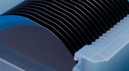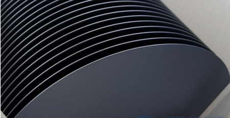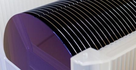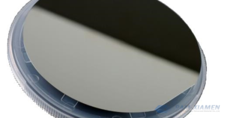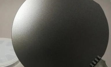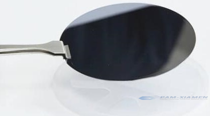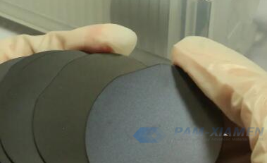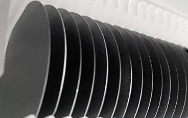
InP / InGaAs Semiconductor Wafer for PIN NIR Diode Detector
Because III-V semiconductor InP / InGaAs has such advantages as direct band structure, high electron mobility, adjustable band gap, long absorption wavelength (920nm~1700nm), it has been widely used in high-speed optoelectronic devices and high-power microwave devices in the near infrared band. Transistors made of InP / InGaAs semiconductor materials overcome the operating limit of 600GHz, improving the bandwidth of frequency devices, and making them have great advantages in high-speed and low-power analog digital hybrid integrated circuits. InGaAs / InP semiconductor wafers are widely used in space remote sensing, process control, radar and night target recognition. GANWAFER is able to provide epi-growth of InP / InGaAs epi layers to fabricate PIN NIR diode detectors. The specific InGaAs wafer structure as follows:
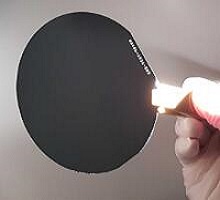
1. Specifications of 3inch InP / InGaAs Semiconductor Wafer
No.1 InGaAs / InP Epitaxy GANW190717-PIN
| Layer Material | Doping | Thickness |
| InP, protective capping layer | intrinsic | – |
| P++ InGaAs | – | ~70nm |
| InP | – | – |
| InGaAs | – | – |
| InP | – | 100nm |
| n- InP | n doped | – |
| n++ InGaAs | – | – |
| InP Substrate | n+ doped |
No.2 InP Wafer with Epilayers for Planar Arrays of Detectors GANW210902 – PIN
| Layer No. | Layer Name | Material | Thickness (um) | Doping (cm-3) |
| 7 | Contact layer | p-InGaAs | – | – |
| 6 | p-InP | 1.0 | – | |
| 5 | p-InP | – | 2 x 10¹⁸ | |
| 4 | Etch stop | p-Q1.3 | – | – |
| 3 | Cladding layer | p-InP | – | – |
| 2 | Active layer | i-Q1.55 | – | – |
| 1 | Buffer layer | n-InP | – | 3 x 10¹⁸ |
| 0 | Substrate | n-InP |
2. Why Grow PIN Type Detectors on InGaAs / InP Structure?
The reasons for growing PIN type detectors based on InGaAs semiconductor epitaxial wafer mainly are:
1) High quantum efficiency in InGaAs / InP epitaxy: The strong electric field in the InGaAs absorption region can make the photogenerated carriers separate and drift quickly, reducing the recombination probability of photogenerated carriers;
2) The absorption efficiency of PIN photodiode can be improved by changing the thickness of I layer during InGaAs semiconductor growth. When the I layer of PIN photodiode is thicker and the doping is lower, the width of the indium gallium arsenide absorption layer is almost equal to the thickness of I layer;
3) It has high sensitivity and low power consumption. Compared with photoconductive detector, PIN photodiode has low dark current and can detect weak signals. In addition, in the PIN junction, because the area with the built-in electric field (type I layer) is wide, the incident light can be almost completely absorbed by the type I layer and converted into photogenerated carriers. Therefore, when the PIN junction InGaAs semiconductor diode is used as a photodetector, it can obtain greater detection sensitivity.
For more information, please contact us email at sales@ganwafer.com and tech@ganwafer.com.