VCSEL Epi Wafer on GaAs / InP Substrate
Ganwafer, as a manufacturer focusing on the research and development, production and sales of compound semiconductor epitaxial stack wafers, includes InP and GaAs-based optoelectronic products. We can provide high-performance VCSEL (Vertical Cavity Surface Emitting Laser) epi wafer grown on GaAs or InP by MBE or MOCVD for the optical communication and intelligent sensing industries. In addition, we accept customized epi-structures for VCSEL. The VCSEL product technology reaches global level. More specifications of VCSEL epi wafer please refer to the following part.
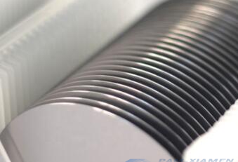
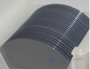
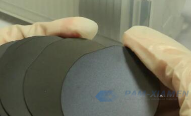
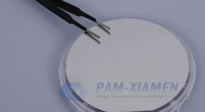
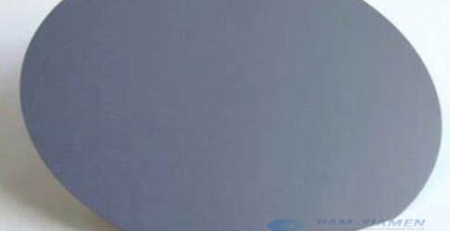
1. Specifications of VCSEL Epi Wafer
The series of products fabricated on VCSEL epi-wafer currently produced can be widely used in optical communications, consumer electronics, industry, automotive, industry and other fields. The VCSEL laser wafers from Ganwafer include:
No.1 GaAs based 850nm/905nm/940nm VCSEL epitaxial wafer: used for optical communication, lidar, 3D sensing (mobile phone);
No.2 GaAs based 808nm/9XXnm/980nm VCSEL semiconductor laser epi-wafer: used in industry, marking, medical treatment, and ranging;
No.3 GaAs based 650nm/680nm/795nm VCSEL epi wafer: used for industrial sensing and atomic clocks;
No.4 Inp based 1.3um/1.5um laser and detector (PIN, APD) epitaxial wafer: used for optical communication.
2. VCSEL Epitaxial Growth
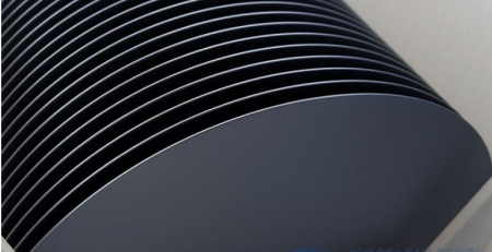
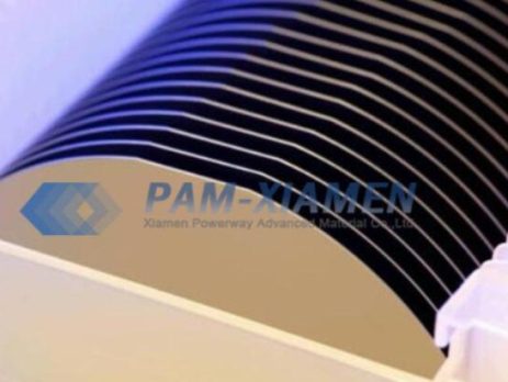
VCSEL epi structure is mainly composed of an active layer that generates photons and a distributed Bragg reflector (DBR). The active layer is sandwiched between the upper and lower distributed Bragg reflectors to form a sandwich-like structure. It requires very high epitaxial growth quality. The photons generated by the active layer reflect back and forth in the upper and lower two distributed Bragg mirrors to produce a resonance effect, and finally amplify and form laser light. Each distributed Bragg reflector is composed of many epitaxial layers, and the refractive index and thickness of each epitaxial layer are customized to cause constructive interference to generate light waves of the desired wavelength.
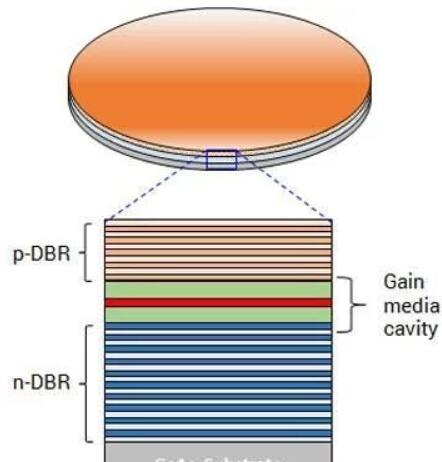
Schematic Diagram of VCSEL Structure
Modulation of the distribution of doping and the uniformity of the composition are crucial in determining the final performance of the device. DBR uniformity of the VCSEL epitaxy determines the wavelength yield of the device itself. Mass-produced 6-inch VCSEL epitaxial wafers need to ensure a wavelength uniformity of about 1 nm to stably control the wavelength of the product. The production of a high-yield VCSEL laser needs to control 6-inch particles/defects within 100 to ensure a surface yield of more than 99%.
Unlike 850nm VSCEL laser diode epi-wafer, which is widely used in the field of optical communications, 940nm VSCEL epi wafer is quite different from the former in terms of semiconductor element composition, and this difference is reflected in the mass production process of epitaxial wafers. The InGaAs/AlGaAs multi-quantum well is the most suitable light-emitting layer material for VCSEL epi-structure, just like the LED uses indium to modulate the wavelength.
The biggest difficulty lies in how to ensure that the structure of each layer of the VSCEL epitaxial wafer can maintain uniform growth. From the structural point of view, the epitaxial growth of a VSCEL device generally has to reach 300 layers, and each layer including the intermediate quality needs to be made very uniform on the process level. In order to ensure the quality of each VCSEL epitaxial layer, the epitaxial growth process needs to be precisely refined to the thickness of each epitaxial layer, and fully modulate the doping distribution and composition under the condition of dozens of times the conventional LED operating current density. Uniformity allows it to grow high-quality low-defect density crystals to obtain high-performance, long-life VCSEL wafer.
3. Comparison with Edge-Emitting Laser and Light-Emitting Diode
Compared with edge-emitting laser (EEL) and light-emitting diode (LED) technologies, the overall advantages of VCSEL are good beam quality, low cost, small size, and easy process integration. In addition, VCSEL also has the advantage of high wavelength stability in the operating temperature range, and can be directional focusing to maximize output efficiency. Because VCSEL is top-emitting (LED is also top-emitting), it can be tested on a wafer, can be integrated with optical devices, and mounted on a printed circuit board (PCB) as a bare VCSEL chip, or package with lasers, drivers, and control logic circuits. Although power output of laser fabricated on VCSEL epi wafer is smaller than that on EEL epitaxial wafer, it can be expanded by creating VCSEL arrays.
With the improvement of VCSEL epitaxy yield and cost control, more and more application light sources choose VCSEL. VCSEL epi wafer is the core technology in the fields of Internet of Things, smart home, unmanned driving, and gesture recognition. VCSEL technology will also become the choice for stability and low-power applications. In addition to consumer-grade devices, VCSEL epi wafer also has broad application prospects in the automotive industry.
For more information, please contact us email at sales@ganwafer.com and tech@ganwafer.com.