InGaAsP Laser Epitaxial Structure in 2004nm Long Wavelength
In1-xGaxAsyP1-y (indium gallium arsenide phosphide) is an alloy material of GaAs, GaP, InAs or InP. The band gap of InGaAsP can change through adjusting the alloy mole ratios of x and y. So this compound can apply in photonics devices. For the InGaAsP / InP material system, lattice mismatch of InGaAsP on InP substrate will make light emission wavelength extend to more than 2 um. The InP / InGaAsP laser epitaxial wafer can be offered by Ganwafer, and the PL tolerance is ± 30 nm. Take the 2004 nm LD III-V epi structure with InGaAs / InGaAsP laser quantum well (QW) for example:
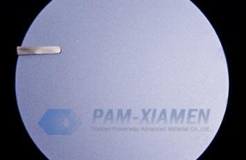
1. 2 inch InGaAsP Laser Structures
GANW220314-LD
| Layer | Material | Thickness (nm) | Dopant | Type |
| 6 | InP | – | Zinc | P |
| 5 | GaIn(x)As | – | Zinc | P |
| 4 | GaIn(x)As(y)P | 30 | Zinc | P |
| 3 | InP | – | Zinc | P |
| 2 | GaInAs/GaInAsP MQW
PL 1960~2010nm |
– | Undoped | U/D |
| 1 | InP Buffer | – | Silicon | N |
| InP Substrate |
2. InGaAsP / InP Heterostructure System
For the InGaAsP / InP material system, the emission wavelength of the material matched with the InP lattice is 1.1-1.65 um. After adding strain in active region, the emission wavelength of InGaAsP / InP heterostructure wafers can reach 2.0 um, which is widely used in laser gas sensing. In addition, InP / InGaAsP thin film epitaxial layer can also be used in infrared detectors, fourth-generation low-light night vision devices and other fields. Recently, the application of this material system to develop surface-emitting lasers, RCLEDs and superluminescent diodes has attracted much attention.
However, as the wavelength increases, the stress caused by the high mismatch causes the lattice relaxation, from two-dimensional growth to three-dimensional growth, and the indium atoms are easily migrated to form In-rich “islands”. Such a problem will make InGaAsP / InGaAs quantum well cannot be applied. To solve this problem, many material growth methods have been developed and many device structures have been designed.
3. Solutions for Avoiding In-rich “Island”
The growth of large-strain InGaAs/InGaAsP quantum wells is the key technology for the fabrication of long-wavelength semiconductor lasers. Therefore, the growth conditions of quantum wells should be optimized before growing the laser structure. Here are some suggestions from literature:
3.1 Optimize Growth Temperature for InGaAs / InGaAsP Quantum Well
The optimum growth temperature for MOCVD growth of InGaAs / InGaAsP laser quantum wells is around 550°C, which can effectively reduce the segregation of In atoms, but for the growth of other epitaxial layers of InGaAsP, this temperature is too low to be used.
Another method is to grow other epitaxial layers at a higher temperature, only the InGaAs epitaxial layer grows at a low temperature.
3.2 Improve Pressure during InGaAs / InGaAsP Laser Diode Epitaxial Growth
The ideal growth pressure for InGaAsP semiconductor laser epitaxial wafer is 22mbar, which helps to speed up the gas switching and make the interface of the epitaxial layer flat; reduce the pre-reaction of the raw materials; create a stable airflow over the surface of the disc.
3.3 Growth Interruption in Epitaxial of InGaAs / InGaAsP QW on InP
The research group of M.Weyers proposed the theory of growth interruption. The growth interruption of 5-10s was added to the growth InP buffer layer. The results of PL showed that: after the growth interruption was added, the luminescence intensity of InGaAsP laser diodes became stronger, the luminescence peak became narrower, and the growth of 5-10s interruptions can smooth out the quantum well heterojunction.
For more information, please contact us email at sales@ganwafer.com and tech@ganwafer.com.