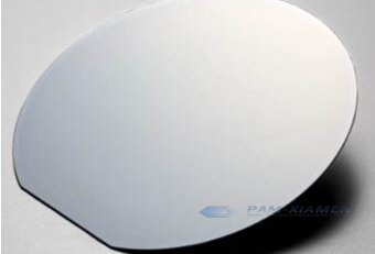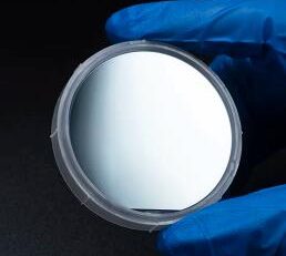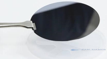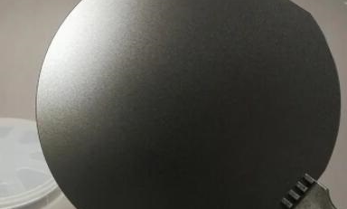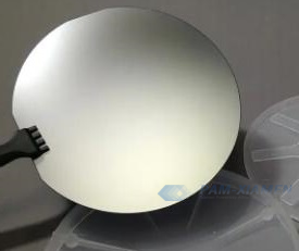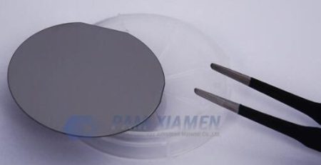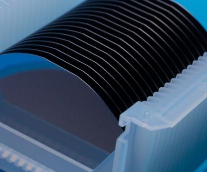
Indium Gallium Arsenide Phosphide (InGaAsP) Thin Film
The indium gallium arsenide phosphide (GalnAsP) quaternary alloy semiconductor material matched with indium phosphide (InP) single crystal substrate lattice has an adjustable band gap range of 0.75~1.35eV. Because the indium gallium arsenide phosphide energy gap covers the low loss bands of 1.33um and 1.55um for quartz fiber signal transmission in current optical communication, it is often used in the structure of indium phosphide heterogeneous junction bipolar transistor, vertical cavity surface emission laser and other optoelectronic devices. Ganwafer is able to provide III-V epitaxial wafer of InP/InGaAsP and grow custom structure. Specific structures are as follows:
1. Specifications of Indium Gallium Arsenide Phosphide Wafer
No. 1 InP based InGaAsP Wafer
GANW190513-INGAASP
| Epi-Layer | Material | Dopant | Thickness | |
| Epi-layer 7 | InP | undoped | – | |
| Epi-layer 6g | InGaAsP | – | 75nm | – |
| Epi-layer 6f | InGaAsP | – | – | – |
| Epi-layer 6e | InGaAsP | – | – | – |
| Epi-layer 6d | InGaAsP | – | – | lattice matched, emitting at 1275 nm |
| Epi-layer 6c | InGaAsP | – | – | – |
| Epi-layer 6b | InGaAsP | – | – | – |
| Epi-layer 6a | InGaAsP | – | – | – |
| Epi-layer 5 | InP | – | – | |
| Epi-layer 4g | InGaAsP | – | 75nm | – |
| Epi-layer 4f | InGaAsP | undoped | – | – |
| Epi-layer 4e | InGaAsP | – | – | – |
| Epi-layer 4d | InGaAsP | – | – | – |
| Epi-layer 4c | InGaAsP | – | – | – |
| Epi-layer 4b | InGaAsP | – | – | – |
| Epi-layer 4a | InGaAsP | – | – | lattice matched, emitting at 1000 nm |
| Epi-layer 3 | InP | – | – | |
| Epi-layer 2g | InGaAsP | – | – | – |
| Epi-layer 2f | InGaAsP | – | – | – |
| Epi-layer 2e | InGaAsP | – | – | – |
| Epi-layer 2d | InGaAsP | – | – | – |
| Epi-layer 2c | InGaAsP | – | 10nm | – |
| Epi-layer 2b | InGaAsP | – | – | |
| Epi-layer 2a | InGaAsP | undoped | – | lattice matched, emitting at 1000 nm |
| Epi-layer 1 | InP | undoped | 300nm | |
| Substrate | InP:S[100], Nc = (3-8)E18/cc, EPD < 5000/cm2 |
No.2 InGaAsP / InP Epiwafers
GANW190709-InGAASP
| Epi-Layer | Material | Dopant | Thickness | |
| Epi-layer 7 | InP | undoped | – | |
| Epi-layer 6g | InGaAsP | – | – | – |
| Epi-layer 6f | InGaAsP | – | 5nm | – |
| Epi-layer 6e | InGaAsP | – | – | – |
| Epi-layer 6d | InGaAsP | – | – | – |
| Epi-layer 6c | InGaAsP | – | – | lattice matched, emitting at 1040 nm |
| Epi-layer 6b | InGaAsP | – | – | – |
| Epi-layer 6a | InGaAsP | – | – | – |
| Epi-layer 5 | InAlAs | – | – | |
| Epi-layer 4g | InGaAsP | – | – | – |
| Epi-layer 4f | InGaAsP | undoped | 5nm | – |
| Epi-layer 4e | InGaAsP | – | – | – |
| Epi-layer 4d | InGaAsP | – | – | – |
| Epi-layer 4c | InGaAsP | – | – | – |
| Epi-layer 4b | InGaAsP | – | – | lattice matched, emitting at 1350 nm |
| Epi-layer 4a | InGaAsP | – | 75nm | – |
| Epi-layer 3 | InAlAs | – | – | |
| Epi-layer 2g | InGaAsP | – | – | – |
| Epi-layer 2f | InGaAsP | – | 5nm | – |
| Epi-layer 2e | InGaAsP | – | – | – |
| Epi-layer 2d | InGaAsP | – | – | – |
| Epi-layer 2c | InGaAsP | – | – | – |
| Epi-layer 2b | InGaAsP | – | – | |
| Epi-layer 2a | InGaAsP | undoped | – | lattice matched, emitting at 1040 nm |
| Epi-layer 1 | InP | undoped | 300nm | |
| Substrate | InP:S[100], Nc = (3-8)E18/cc, EPD < 5000/cm2 |
No. 3 InGaAsP Quantum Well Structure
GANW190527-INGAASP
| Epi-Layer | Material | Dopant | Thickness | |
| Epi-layer 11 | n-InP capping layer | Si | – | |
| Epi-layer 10 | n-1.24Q InGaAsP, delta doping | – | – | |
| Epi-layer 9 | i-1.24Q InGaAsP | – | – | |
| Epi-layer 8 | 1.30Q (-0.5%) InGaAsP barrier | – | – | λc=1.55um |
| Epi-layer 7 | 1.65Q (+0.8%) InGaAsP well | – | – | |
| Epi-layer 6 | 1.30Q (-0.5%) InGaAsP barrier | – | – | |
| Epi-layer 5 | i-1.24Q InGaAsP | – | 300A | |
| Epi-layer 4 | p-1.24Q InGaAsP | Zn | – | |
| Epi-layer 3 | p-InP sacrificial layer | – | – | |
| Epi-layer 2 | p-InGaAs etch-stop layer | – | 0.4um | |
| Epi-layer 1 | p-buffer InP | – | – | |
| Substrate | p-InP |
2. FAQ of InGaAsP Wafer
Q1: I have a technical question:
Do you know if InGaAsP with bandgap at 950 nm is resistant to concentrated HCl (hydrochloric acid)?
A: The corrosion for indium gallium arsenide phosphide crystal wafer may be irresistible, but the corrosion rate should be slower.
Q2: I have received your InGaAsP wafer with FWHM 54.5nm (see attached). Is it possible to provide InGaAsP wafer with narrower FWHM (less than 54.5nm)? Possible to 30nm? Or 20nm?
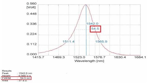
A: It’s no problem for manufacturing GaInAsP epi wafer with FWHM<54.5nm and what we can guarantee is near 30nm.
Q3: I have used your InGaAsP heterostructure as well as other wafers to make a nano-material light emitting source. Compared with the device made InGaAsP wafer from another company, the device based on your wafer was shown that the average voltage was low, even though put more power (35 vs. 350 μW).
Could you please give us an explanation/opinion about the comparison test result?
A: The difference of GaInAsP epitaxy on P-type InP may be due to the difference of doping concentration between P-type and N-type. We are in accordance with the concentration of your requirements. It is clear that the doping concentration is too high, the optical absorption loss is very large, not structural problem. PL can be much stronger if the doping point is lower. This phenomenon is obviously related to doping.
For more information, please contact us email at sales@ganwafer.com and tech@ganwafer.com.