GaInP/AlInP Leuchtdiodenstruktur
Light emitting diode (LED) structure with GaInP / AlInP epilayers can be offered by Ganwafer. The ternary InGaP and AlInP materials are lattice matched to GaAs susbtrate, which can be grown by MOCVD. Growing high quality Ternäres III-V-Halbleitermaterial is important to the fabrication of light emitting diodes, laser diodes and multi-junction photovoltaic. Light emitting diode structure with ternary GaInP and AlInP epilayers from Ganwafer is shown as follows:
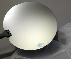
1. GaAs-Epi-Struktur einer Leuchtdiode
No.1 GaAs LED Epitaxy
|
GaAs LED Structure (GANWP20065-LED) |
||
| Schichtmaterial | Dicke | Notiz |
| p-GaInP | - - | Composition of In: 0.5;
Mg-dotiert |
| p-GaP | - - | |
| p-AlInP | - - | |
| MQW | - - | |
| n-AlInP | - - | |
| DBR | - - | |
| Ätzstopp n-GaInP | 20nm | |
| Pufferschicht | - - | |
| GaAs-Subst. | 350 um | |
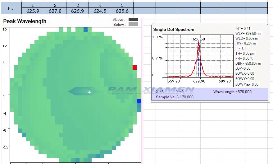
Der PL- und El-Test des Quanten-Leuchtdiodenwafers ist als Diagramm dargestellt:
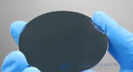
No. 2 GaAs based InGaP LED Epitaxy Wafer
GANW190724-INGAP
| Layer Name | Material | Dicke |
| P-cladding layer | P-AlInP | - - |
| Active layer | MQW | - - |
| N-cladding layer | N-AlInP | 900nm |
| Bragg reflector | N-AlGaAs/AlAs | - - |
| Pufferschicht | N-GaAs | |
| Substrat | N-GaAs on-axis (100) plane without offcut |
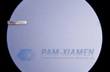
No. 3 GaAs based LED Epitaxial Structure
GANWP19168-INGAP
| Layer Name | Material | Dicke |
| P-cladding layer | P-AlInP | - - |
| Active layer | MQW | - - |
| N-cladding layer | N-AlInP | - - |
| Pufferschicht | N-GaAs | 300nm |
| Substrat | N-GaAs on-axis (100) plane without offcut |
2. FAQ of GaAs Light Emitting Diode Wafer
Q:We observed two MQW regions in GaInP LED wafer (GANWP19168-INGAP), illustrated in below figure. There are 9 pairs in each MQW separated by a thick barrier layer. May I know any reason to grow this kind of structure instead of a single stack of MQWs?
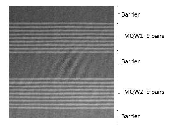
A: These are two groups of identical quantum wells in InGaP LED epitaxy. In order to increase the thickness of the active region and improve the reliability of the LED chip, the middle layer can be used normally without any influence on the photoelectric performance.
3. InGaP on GaAs for Light Emitting Diode Structure
InGaP, das ein großes Potenzial zum Ersatz der aluminiumhaltigen Materialien aufweist, ist ein kritisches Halbleitermaterial, das normalerweise auf einem GaAs-Substrat gezüchtet wird. Seine Eigenschaften hängen eng mit den Wachstumsbedingungen wie Wachstumsmethode, Substrattemperatur, Wachstumsrate, Substratorientierung, III/V-Verhältnis usw. zusammen. Daher ist InGaP ideal für das Wachstum von Heterostrukturen für verschiedene Anwendungen, wie z. B. rote LEDs mit hoher Helligkeit.
Die Attraktivität der InGaP/GaAs-Heterostruktur ergibt sich aus ihrer Bandausrichtung, der Valenzband-Offset (AEv = 0,24 – 0,40 eV) ist deutlich größer als der Leitungsband-Offset (Mc = 0,03 – 0,22 eV). Dies wird als günstiger angesehen als die Bandstruktur des AlGaAs/GaAs-Heterosystems.
InGaP ist ein hochselektives Ätzen von GaAs, das als Ätzstoppschicht in unserer epitaxialen LED-Struktur verwendet wird. Dies wird die Formfähigkeit und Herstellbarkeit von lichtemittierenden Diodenmikrovorrichtungen erhöhen. Aber die GaInP-Ätzstoppschicht erhöht die Höhe der Energiebarriere, die überwunden werden muss, wenn Elektronen vom Kollektor zum Subkollektor fließen. Unter dieser Bedingung nimmt die Gleichstromverstärkung der MQW-LED-Struktur ab. Daher sollte die Ätzstoppschicht aus InGaP dünn genug sein, um die Geräteleistung sicherzustellen.
Für weitere Informationen kontaktieren Sie uns bitte per E-Mail unter sales@ganwafer.com und tech@ganwafer.com.