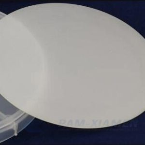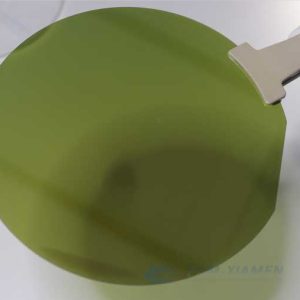
GaN auf Saphir-HEMT-Wafer

Ganwafer offers GaN on Sapphire wafers with HEMT structure and GaN template on Sapphire substrate for power or RF devices. The epitaxial layers of GaN based materials and devices are mainly grown on sapphire substrates. Why epitaxial GaN growth on Sapphire? Reasons are that sapphire substrate has many advantages: firstly, sapphire substrate has mature production technology and good device quality; secondly, sapphire has good stability and can be used in high temperature growth process; finally, sapphire has high mechanical strength and is easy to handle and clean. Therefore, most of the GaN HEMT wafer processes are based on sapphire. However, using sapphire as substrate also has some problems, such as lattice mismatch and thermal stress mismatch, which will produce a large number of defects in the GaN / Sapphire epitaxial layer and cause difficulties in the subsequent device processing.
Und jetzt sehen Sie bitte unten GaN-on-Sapphire-HEMT-Wafer-Spezifikationen:
- Beschreibung
- Anfrage
Beschreibung
1. GaN auf Saphirwafer mit HEMT-Struktur für Leistungsanwendungen
| Wafergröße | 2", 3", 4", 6" |
| AlGaN / GaN HEMT-Struktur | siehe 1.2 |
| Trägerdichte | 6E12~2E13 cm2 |
| Hallenmobilität | /. |
| XRD(102)FWHM | ~Bogen.Sek |
| XRD(002)FWHM | ~Bogen.Sek |
| Blattwiderstand | /. |
| AFM RMS (nm) von 5x5um2 | <0,25 nm |
| Schleife (ähm) | <=35um |
| Randausschluss | <2mm |
| SiN-Passivierungsschicht | 0~30nm |
| Al-Zusammensetzung | 20-30% |
| In Komposition | 17 % für InAlN |
| GaN-Kappe | /. |
| AlGaN/(In)AlN-Barriere | /. |
| AlN-Zwischenschicht | /. |
| GaN-Kanal | /. |
| C-dotierter GaN-Puffer | /. |
| Nacktheit | /. |
| Substratmaterial | Saphirsubstrat |
2. GaN-HEMT-Struktur auf Saphirsubstrat für HF-Anwendung
| Wafergröße | 2", 3", 4", 6" |
| AlGaN / GaN HEMT-Struktur | siehe 1.2 |
| Trägerdichte | 6E12~2E13 cm2 |
| Hallenmobilität | /. |
| XRD(102)FWHM | /. |
| XRD(002)FWHM | /. |
| Blattwiderstand | /. |
| AFM RMS (nm) von 5x5um2 | <0,25 nm |
| Schleife (ähm) | <=35um |
| Randausschluss | <2mm |
| siN-Passivierungsschicht | 0~30nm |
| u-GaN-Deckschicht | /. |
| Al-Zusammensetzung | 20-30% |
| In Komposition | 17 % für InAlN |
| AlGaN-Sperrschicht | 20~30nm |
| AlN-Abstandshalter | /. |
| GaN-Pufferschicht (um) | /. |
| GaN-Kanal | /. |
| Fe-dotierter GaN-Puffer | /. |
| Nacktheit | /. |
| Substratmaterial | Saphirsubstrat |
Anmerkung:
Die chinesische Regierung hat neue Beschränkungen für den Export von Galliummaterialien (wie GaAs, GaN, Ga2O3, GaP, InGaAs und GaSb) und Germaniummaterialien zur Herstellung von Halbleiterchips angekündigt. Ab dem 1. August 2023 ist der Export dieser Materialien nur noch erlaubt, wenn wir eine Lizenz des chinesischen Handelsministeriums erhalten. Hoffe auf ihr Verständnis!