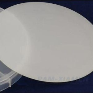
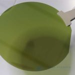
サファイアHEMTウェーハ上のGaN

Ganwafer offers GaN on Sapphire wafers with HEMT structure and GaN template on Sapphire substrate for power or RF devices. The epitaxial layers of GaN based materials and devices are mainly grown on sapphire substrates. Why epitaxial GaN growth on Sapphire? Reasons are that sapphire substrate has many advantages: firstly, sapphire substrate has mature production technology and good device quality; secondly, sapphire has good stability and can be used in high temperature growth process; finally, sapphire has high mechanical strength and is easy to handle and clean. Therefore, most of the GaN HEMT wafer processes are based on sapphire. However, using sapphire as substrate also has some problems, such as lattice mismatch and thermal stress mismatch, which will produce a large number of defects in the GaN / Sapphire epitaxial layer and cause difficulties in the subsequent device processing.
そして今、以下のGaN-on-SapphireHEMTウェーハの仕様をご覧ください。
- 説明
- 問い合わせ
説明
1.電力アプリケーション用のHEMT構造を備えたサファイアウェーハ上のGaN
| ウェーハサイズ | 2” 、3” 、4” 、6” |
| AlGaN / GaN HEMT構造 | 1.2を参照してください。 |
| キャリア密度 | 6E12〜2E13 cm2 |
| ホール移動度 | / |
| XRD(102)FWHM | 〜arc.sec |
| XRD(002)FWHM | 〜arc.sec |
| シート抵抗率 | / |
| 5x5um2のAFMRMS(nm) | <0.25nm |
| ボウ(UM) | <= 35um |
| エッジ除外 | <2ミリメートル |
| SiNパッシベーション層 | 0〜30nmで |
| Al組成 | 20から30パーセント |
| 組成物において、 | InAlNを17% |
| GaNキャップ | / |
| AlGaN /(IN)のAlN障壁 | / |
| AlN中間層 | / |
| GaNチャネル | / |
| Cは、GaNバッファドープ | / |
| Nudeation | / |
| 基板材料 | サファイア基板 |
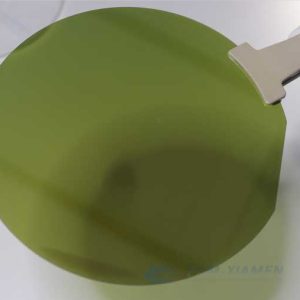
2.RFアプリケーション用のサファイア基板上のGaNHEMT構造
| ウェーハサイズ | 2” 、3” 、4” 、6” |
| AlGaN / GaN HEMT構造 | 1.2を参照してください。 |
| キャリア密度 | 6E12〜2E13 cm2 |
| ホール移動度 | / |
| XRD(102)FWHM | / |
| XRD(002)FWHM | / |
| シート抵抗率 | / |
| 5x5um2のAFMRMS(nm) | <0.25nm |
| ボウ(UM) | <= 35um |
| エッジ除外 | <2ミリメートル |
| siNパッシベーションレイヤー | 0〜30nmで |
| u-GaNキャップ層 | / |
| Al組成 | 20から30パーセント |
| 組成物において、 | InAlNを17% |
| AlGaNバリア層 | 20〜30nm |
| AlNスペーサー | / |
| GaNバッファ層(um) | / |
| GaNチャネル | / |
| FEは、GaNバッファドープ | / |
| Nudeation | / |
| 基板材料 | サファイア基板 |
述べる:
中国政府は、半導体チップの製造に使用されるガリウム材料(GaAs、GaN、Ga2O3、GaP、InGaAs、GaSbなど)およびゲルマニウム材料の輸出に対する新たな制限を発表しました。 2023 年 8 月 1 日以降、これらの材料の輸出は中国商務省から許可を取得した場合にのみ許可されます。 ご理解いただければ幸いです。