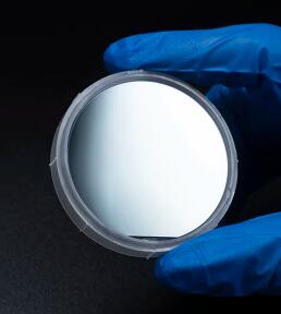
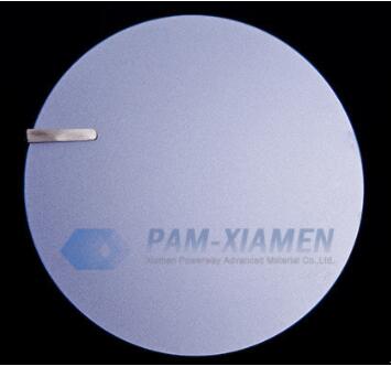
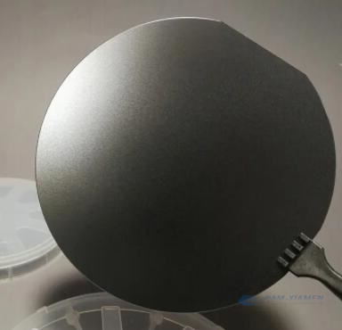
GaN/Si-HEMT-Struktur
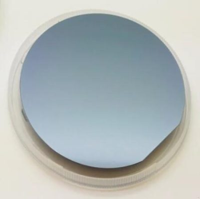
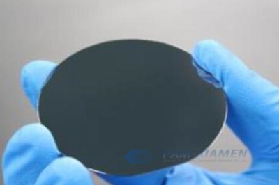
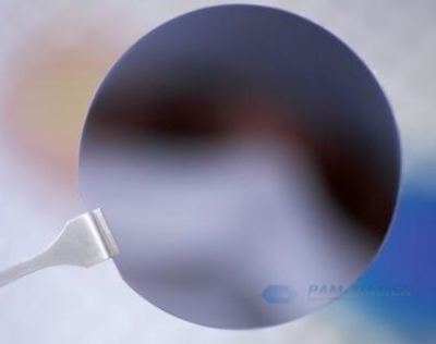
GaN has excellent physical properties such as high breakdown electric field strength and high thermal conductivity, making it an ideal material for fabricating high-frequency...

GaN has excellent physical properties such as high breakdown electric field strength and high thermal conductivity, making it an ideal material for fabricating high-frequency...
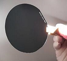
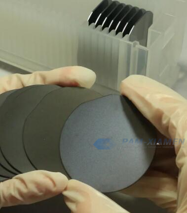
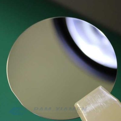
Indium antimonide (InSb), as a III-V binary compound semiconductor material, has stable physical and chemical properties and excellent process compatibility. InSb has a very narrow...
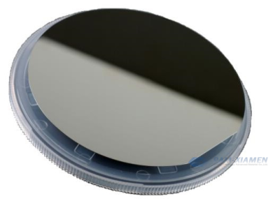
Using bulk materials and quantum wells as active regions, InP-based material systems can cover all wavelengths of optical fiber communication. At present, materials used...
Because III-V semiconductor InP / InGaAs has such advantages as direct band structure, high electron mobility, adjustable band gap, long absorption wavelength (920nm~1700nm), it...
The indium gallium arsenide phosphide (GalnAsP) quaternary alloy semiconductor material matched with indium phosphide (InP) single crystal substrate lattice has an adjustable band gap...
LED epitaxial wafers are located in the upstream link of the LED industry chain, which is the link with the highest technical content in...
As a leading semiconductor wafer manufacturer, Ganwafer can supply III-V semiconductor epitaxial wafers, more specifications please refer to https://www.ganwafer.com/product/iii-v-epi-wafer/. Here we take the delta...
In terms of mid-infrared detection in the 3-5um band, detectors based on InSb materials stand out from many material devices due to their mature...
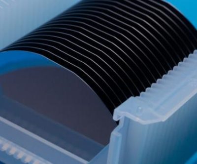
We often receive the demands for “wafer”, “die”, and “chip” from customers. Among them, what Ganwafer can offer is the semiconductor wafer. So what...
Ganwafer can supply GaAs based LED wafer with GaInP / AlGaInP multi-quantum wells (MQWs). There are two categories of LEDs used in the lighting...
Metal-organic chemical vapor deposition (MOCVD) is a new vapor phase epitaxy growth technology developed on the basis of vapor phase epitaxy (VPE). MOCVD uses...
Indium antimonide (InSb) has the characteristics of the lowest melting point, narrow band gap, high carrier mobility, and good structural integrity. It is a...