GaSb-Wafer
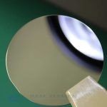
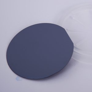
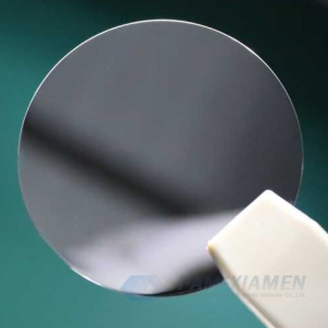
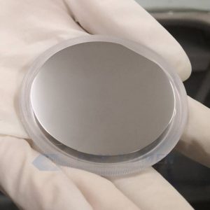
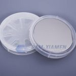
Gallium antimonide (GaSb) material from Ganwafer a gallium antimonide wafer supplier is an important substrate material for manufacturing 2~4um lasers, infrared light-emitting tubes and high-speed low-noise avalanche photodiodes. Its three- and quaternary compound epitaxial growth has good lattice matching, and it is one of the ideal light source materials for manufacturing optical communication devices. Device manufacturing on single crystal GaSb substrate requires the preparation of a stable oxide layer with low interface density, high resistivity, high breakdown voltage and suitable for high-temperature processes. More about GaSb (Gallium Antimonide) crystal substrates please contact us.
- Beschreibung
- Anfrage
Beschreibung
As one of important III–V compound semiconductor materials, gallium antimonide is applied in optoelectronic devices. Because of the gallium antimonide properties, such as high quantum efficiency, high hole mobility, and super lattices with customized optical and transport characteristics, devices fabricated on GaSb substrate is ideal for the mid-infrared (2-5um and 8-14um wavelength) applications, like imaging sensors for fire detection, surveillance system and environmental pollution monitors.
1. 4″ Spezifikation für epitaxiefähige GaSb-Wafer
| Artikel | Technische Daten | ||
| Dotierstoff | niedrig dotiert | Zink | Tellur |
| Conduction Typ | P-Typ | P-Typ | N-Typ |
| Wafer-Durchmesser | 4 " | ||
| Wafer Orientation | (100) ± 0,5 ° | ||
| Waferdicke | 800 ± 25 um | ||
| Primäre Wohnung Länge | 32,5 ± 2,5 mm | ||
| Secondary Wohnung Länge | 18 ± 1 mm | ||
| Ladungsträgerkonzentration | (1-2)x1017cm-3 | (5-100)x1017cm-3 | (1-20)x1017cm-3 |
| Mobilität | 600-700 cm2/Vs | 200-500cm2/Vs | 2000-3500cm2/Vs |
| EPD | <2×103cm-2 | ||
| TTV | <15um | ||
| BOGEN | <15um | ||
| KETTE | <20um | ||
| Laserbeschriftung | auf Anfrage | ||
| Oberflächenfinish | P / E, P / P | ||
| Epi bereit | ja | ||
| Paket | Einzelner Waferbehälter oder Kassette | ||
2. Spezifikation für 3″ Galliumantimonid-Wafer
| Artikel | Technische Daten | ||
| Conduction Typ | P-Typ | P-Typ | N-Typ |
| Dotierstoff | niedrig dotiert | Zink | Tellur |
| Wafer-Durchmesser | 3" | ||
| Wafer Orientation | (100) ± 0,5 ° | ||
| Waferdicke | 600 ± 25 um | ||
| Primäre Wohnung Länge | 22 ± 2mm | ||
| Secondary Wohnung Länge | 11 ± 1mm | ||
| Ladungsträgerkonzentration | (1-2)x1017cm-3 | (5-100)x1017cm-3 | (1-20)x1017cm-3 |
| Mobilität | 600-700 cm2/Vs | 200-500cm2/Vs | 2000-3500cm2/Vs |
| EPD | <2×103cm-2 | ||
| TTV | <12um | ||
| BOGEN | <12um | ||
| KETTE | <15um | ||
| Laserbeschriftung | auf Anfrage | ||
| Oberflächenfinish | P / E, P / P | ||
| Epi bereit | ja | ||
| Paket | Einzelner Waferbehälter oder Kassette | ||
3. Spezifikation des 2″ GaSb (Galliumantimonid)-Wafersubstrats
| Artikel | Technische Daten | ||
| Dotierstoff | niedrig dotiert | Zink | Tellur |
| Conduction Typ | P-Typ | P-Typ | N-Typ |
| Wafer-Durchmesser | 2 " | ||
| Wafer Orientation | (100) ± 0,5 ° | ||
| Waferdicke | 500 ± 25 um | ||
| Primäre Wohnung Länge | 16 ± 2mm | ||
| Secondary Wohnung Länge | 8 ± 1mm | ||
| Ladungsträgerkonzentration | (1-2)x1017cm-3 | (5-100)x1017cm-3 | (1-20)x1017cm-3 |
| Mobilität | 600-700 cm2/Vs | 200-500cm2/Vs | 2000-3500cm2/Vs |
| EPD | <2×103cm-2 | ||
| TTV | <10um | ||
| BOGEN | <10um | ||
| KETTE | <12um | ||
| Laserbeschriftung | auf Anfrage | ||
| Oberflächenfinish | P / E, P / P | ||
| Epi Bereit | ja | ||
| Paket | Einzelner Waferbehälter oder Kassette | ||
Viele Eigenschaften von Halbleitervorrichtungen sind eng mit Eigenschaften einer Halbleiteroberfläche verbunden. Es ist erwähnenswert, dass ein Einkristall-GaSb-Wafer durch atmosphärischen Sauerstoff gebildete natürliche Oberflächenoxide mit einer Dicke von wenigen Nanometern leicht zu oxidieren sind, da er eine sehr hochgradig chemisch reaktive Oberfläche hat.
Anmerkung:
Die chinesische Regierung hat neue Beschränkungen für den Export von Galliummaterialien (wie GaAs, GaN, Ga2O3, GaP, InGaAs und GaSb) und Germaniummaterialien zur Herstellung von Halbleiterchips angekündigt. Ab dem 1. August 2023 ist der Export dieser Materialien nur noch erlaubt, wenn wir eine Lizenz des chinesischen Handelsministeriums erhalten. Hoffe auf ihr Verständnis!