GaN på Sapphire HEMT Wafer

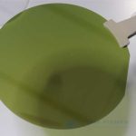
Ganwafer offers GaN on Sapphire wafers with HEMT structure and GaN template on Sapphire substrate for power or RF devices. The epitaxial layers of GaN based materials and devices are mainly grown on sapphire substrates. Why epitaxial GaN growth on Sapphire? Reasons are that sapphire substrate has many advantages: firstly, sapphire substrate has mature production technology and good device quality; secondly, sapphire has good stability and can be used in high temperature growth process; finally, sapphire has high mechanical strength and is easy to handle and clean. Therefore, most of the GaN HEMT wafer processes are based on sapphire. However, using sapphire as substrate also has some problems, such as lattice mismatch and thermal stress mismatch, which will produce a large number of defects in the GaN / Sapphire epitaxial layer and cause difficulties in the subsequent device processing.
Och se nu nedan GaN-on-Sapphire HEMT wafer-specifikationer:
- Beskrivning
- Förfrågan
Beskrivning
1. GaN på Sapphire Wafer med HEMT-struktur för krafttillämpning
| Wafer storlek | 2", 3", 4", 6" |
| AlGaN / GaN HEMT struktur | hänvisa 1,2 |
| Bärardensitet | 6E12~2E13 cm2 |
| Hallrörlighet | / |
| XRD(102)FWHM | ~båge.sek |
| XRD(002)FWHM | ~båge.sek |
| Arkresistivitet | / |
| AFM RMS (nm) på 5x5um2 | <0,25 nm |
| Bow(um) | <=35um |
| Edge uteslutning | <2 mm |
| SiN passiveringsskikt | 0~30nm |
| Al sammansättning | 20-30 % |
| I komposition | 17 % för InAlN |
| GaN lock | / |
| AlGaN/(In)AlN-barriär | / |
| AlN mellanskikt | / |
| GaN-kanal | / |
| C-dopad GaN-buffert | / |
| Nakenbild | / |
| Underlagsmaterial | safirsubstrat |
2. GaN HEMT-struktur på safirsubstrat för RF-applikation
| Wafer storlek | 2", 3", 4", 6" |
| AlGaN / GaN HEMT struktur | hänvisa 1,2 |
| Bärardensitet | 6E12~2E13 cm2 |
| Hallrörlighet | / |
| XRD(102)FWHM | / |
| XRD(002)FWHM | / |
| Arkresistivitet | / |
| AFM RMS (nm) på 5x5um2 | <0,25 nm |
| Bow(um) | <=35um |
| Edge uteslutning | <2 mm |
| siN passiveringsskikt | 0~30nm |
| u-GaN locklager | / |
| Al sammansättning | 20-30 % |
| I komposition | 17 % för InAlN |
| AlGaN barriärskikt | 20~30nm |
| AlN spacer | / |
| GaN-buffertlager(um) | / |
| GaN-kanal | / |
| Fe-dopad GaN-buffert | / |
| Nakenbild | / |
| Underlagsmaterial | safirsubstrat |
Anmärkning:
Den kinesiska regeringen har aviserat nya gränser för export av galliummaterial (som GaAs, GaN, Ga2O3, GaP, InGaAs och GaSb) och germaniummaterial som används för att tillverka halvledarchips. Från och med den 1 augusti 2023 är export av detta material endast tillåtet om vi får en licens från det kinesiska handelsministeriet. Hoppas på din förståelse!