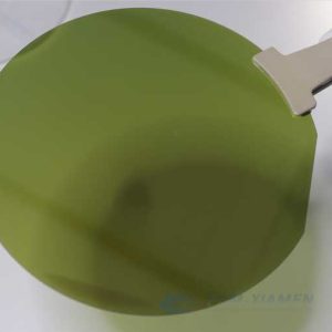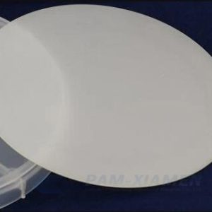
GaN på Silicon HEMT Wafer
Ganwafer offers GaN (Gallium Nitride) on Silicon (Si) Epitaxy HEMT wafer and GaN template on Si substrate. According to different applications, GaN on Silicon HEMT wafer can be classified into GaN-on-Silicon wafer for D-mode, GaN on Silicon substrate for E-mode and GaN on Silicon wafer for RF application. GaN based power electronic devices are still very expensive compared with Si devices. One of the ways to solve the cost problem is to fabricate GaN based heterostructures by epitaxy on Si substrate, and then to fabricate GaN based devices by complementary metal oxide semiconductor (CMOS) technology, so that the cost performance of the devices is better than that of Si devices. However, it is much more difficult to grow GaN on Silicon substrates than on SiC and sapphire substrates. The lattice mismatch ratio of GaN (0001) and Silicon (111) is as high as 16.9%, and the thermal expansion coefficient mismatch (thermal mismatch) is as high as 56%. These are main epitaxial challenges of GaN on Silicon, which may be able to be solved by introducing a buffer layer to GaN on Silicon wafer substrate. As a leading GaN on Silicon HEMT wafer manufacturer, we continuously develop our existing GaN on Silicon technology to gain a better wafer to you. And now please see below GaN on Si wafer specification:
- Beskrivning
- Förfrågan
Beskrivning
1. GaN på Silicon HEMT Wafer, D-LÄGE
1.1 Specifikation av GaN HEMT Wafer on Silicon, D-LÄGE
| Wafer storlek | 2″, 4″, 6″, 8″ |
| AlGaN / GaN HEMT struktur | hänvisa 1,2 |
| Bärardensitet | >9E12 cm2 |
| Hallrörlighet | / |
| Arkresistivitet | / |
| AFM RMS (nm) på 5x5um2 | <0,25 nm |
| Bow(um) | <=30um |
| Edge uteslutning | <5 mm |
| SiN passiveringsskikt | 0~5nm |
| u-GaN locklager | 2 nm |
| Al sammansättning | 20-30 % |
| AlGaN barriärskikt | / |
| GaN-kanal | / |
| AlGaN-buffert | / |
| AIN | / |
| Underlagsmaterial | Silikonsubstrat |
| Si wafer tjocklek (μm) | 675um(2″), 1000um(4″), 1300um(6″), 1500um(8″) |
1.2 Struktur för GaN HEMT Wafer på kisel, D-LÄGE

2. GaN på Silicon HEMT Epitaxi, E-LÄGE
| Wafer storlek | 2″, 4″, 6″, 8″ |
| AlGaN / GaN HEMT struktur | hänvisa 1,2 |
| Återstående 2DEG densitet (Vg=0 V) | <1e18/cm3 |
| AFM RMS (nm) på 5x5um2 | <0,25 nm |
| Bow(um) | <=30um |
| Edge uteslutning | <5 mm |
| p-GaN | / |
| u-GaN locklager | / |
| Al sammansättning | 20-30 % |
| AlGaN barriärskikt | / |
| GaN-kanal | / |
| AlGaN-buffert | / |
| Underlagsmaterial | Silikonsubstrat |
| Si wafer tjocklek (μm) | 675um(2″), 1000um(4″), 1300um(6″), 1500um(8″) |
3. Galliumnitrid HEMT Wafer på kisel för RF-applikation
| Wafer storlek | 2″, 4″, 6″, 8″ |
| AlGaN / GaN HEMT struktur | hänvisa 1,2 |
| Bärardensitet | >9E12 cm2 |
| Hallrörlighet | / |
| Arkresistivitet | / |
| AFM RMS (nm) på 5x5um2 | <0,25 nm |
| Bow(um) | <=30um |
| Edge uteslutning | <5 mm |
| SiN passiveringsskikt | 0~5nm |
| u-GaN locklager | / |
| Al sammansättning | 20-30 % |
| AlGaN barriärskikt | / |
| GaN-kanal | / |
| AlGaN-buffert | / |
| AIN | / |
| Underlagsmaterial | Silikonsubstrat |
| Si-substratresistivitet (Ω cm) | > 3000 |
| Si wafer tjocklek (μm) | 1000um(2″), 1000um(4″), 1300um(6″), 1500um(8″) |
Anmärkning:
Den kinesiska regeringen har aviserat nya gränser för export av galliummaterial (som GaAs, GaN, Ga2O3, GaP, InGaAs och GaSb) och germaniummaterial som används för att tillverka halvledarchips. Från och med den 1 augusti 2023 är export av detta material endast tillåtet om vi får en licens från det kinesiska handelsministeriet. Hoppas på din förståelse!