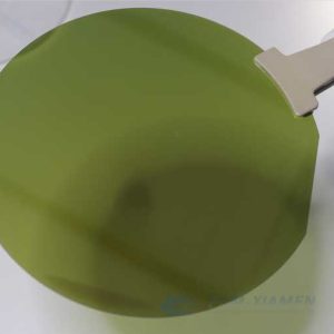
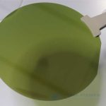
GaN na Sapphire HEMT Wafel

Ganwafer offers GaN on Sapphire wafers with HEMT structure and GaN template on Sapphire substrate for power or RF devices. The epitaxial layers of GaN based materials and devices are mainly grown on sapphire substrates. Why epitaxial GaN growth on Sapphire? Reasons are that sapphire substrate has many advantages: firstly, sapphire substrate has mature production technology and good device quality; secondly, sapphire has good stability and can be used in high temperature growth process; finally, sapphire has high mechanical strength and is easy to handle and clean. Therefore, most of the GaN HEMT wafer processes are based on sapphire. However, using sapphire as substrate also has some problems, such as lattice mismatch and thermal stress mismatch, which will produce a large number of defects in the GaN / Sapphire epitaxial layer and cause difficulties in the subsequent device processing.
A teraz zobacz poniżej specyfikacje płytek GaN-on-Sapphire HEMT:
- Opis
- Zapytanie
Opis
1. GaN na waflu szafirowym ze strukturą HEMT do zastosowań energetycznych
| Rozmiar wafla | 2”, 3”, 4”, 6” |
| Struktura AlGaN / GaN HEMT | patrz 1.2 |
| Gęstość nośna | 6E12~2E13 cm2 |
| Mobilność hali | / |
| XRD(102)FWHM | ~arc.sek |
| XRD(002)FWHM | ~arc.sek |
| Rezystywność arkusza | / |
| AFM RMS (nm) 5x5um2 | <0,25 nm |
| Łuk (um) | <=35um |
| wykluczenie krawędź | <2mm |
| Warstwa pasywacyjna SiN | 0~30nm |
| Skład Al | 20-30% |
| W składzie | 17% dla InAlN |
| Czapka GaN | / |
| Bariera AlGaN/(In)AlN | / |
| warstwa pośrednia AlN | / |
| kanał GaN | / |
| C domieszkowany bufor GaN | / |
| Nagość | / |
| Materiał podłoża | Sapphire podłoże |
2. Struktura GaN HEMT na podłożu szafirowym do zastosowań RF
| Rozmiar wafla | 2”, 3”, 4”, 6” |
| Struktura AlGaN / GaN HEMT | patrz 1.2 |
| Gęstość nośna | 6E12~2E13 cm2 |
| Mobilność hali | / |
| XRD(102)FWHM | / |
| XRD(002)FWHM | / |
| Rezystywność arkusza | / |
| AFM RMS (nm) 5x5um2 | <0,25 nm |
| Łuk (um) | <=35um |
| wykluczenie krawędź | <2mm |
| SiN warstwa pasywacyjna | 0~30nm |
| warstwa nasadki u-GaN | / |
| Skład Al | 20-30% |
| W składzie | 17% dla InAlN |
| Warstwa barierowa AlGaN | 20~30nm |
| przekładka AlN | / |
| Warstwa buforowa GaN (um) | / |
| kanał GaN | / |
| Bufor GaN domieszkowany Fe | / |
| Nagość | / |
| Materiał podłoża | Sapphire podłoże |
Uwaga:
Chiński rząd ogłosił nowe ograniczenia eksportu materiałów galu (takich jak GaAs, GaN, Ga2O3, GaP, InGaAs i GaSb) oraz materiałów germanu używanych do produkcji układów półprzewodnikowych. Od 1 sierpnia 2023 r. eksport tych materiałów jest dozwolony tylko po uzyskaniu licencji chińskiego Ministerstwa Handlu. Liczę na twoje zrozumienie!