GaN pada Wafer HEMT Nilam

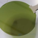
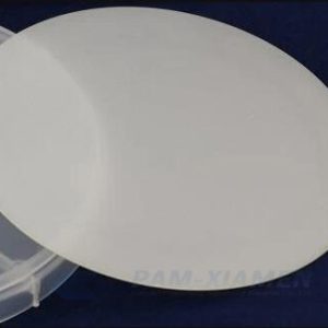
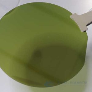
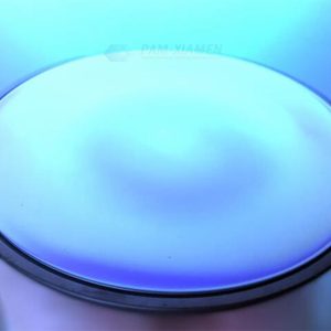
Ganwafer offers GaN on Sapphire wafers with HEMT structure and GaN template on Sapphire substrate for power or RF devices. The epitaxial layers of GaN based materials and devices are mainly grown on sapphire substrates. Why epitaxial GaN growth on Sapphire? Reasons are that sapphire substrate has many advantages: firstly, sapphire substrate has mature production technology and good device quality; secondly, sapphire has good stability and can be used in high temperature growth process; finally, sapphire has high mechanical strength and is easy to handle and clean. Therefore, most of the GaN HEMT wafer processes are based on sapphire. However, using sapphire as substrate also has some problems, such as lattice mismatch and thermal stress mismatch, which will produce a large number of defects in the GaN / Sapphire epitaxial layer and cause difficulties in the subsequent device processing.
Dan sekarang sila lihat di bawah spesifikasi wafer HEMT GaN-on-Sapphire:
- Penerangan
- Siasatan
Penerangan
1. GaN pada Wafer Nilam dengan Struktur HEMT untuk Aplikasi Kuasa
| Saiz wafer | 2”, 3”, 4”, 6” |
| struktur AlGaN / Gan HEMT | rujuk 1.2 |
| Ketumpatan pembawa | 6E12~2E13 sm2 |
| Mobiliti dewan | / |
| XRD(102)FWHM | ~arc.sec |
| XRD(002)FWHM | ~arc.sec |
| Kerintangan Lembaran | / |
| AFM RMS (nm) sebanyak 5x5um2 | <0.25nm |
| Tunduk(um) | <=35um |
| pengecualian Edge | <2mm |
| Lapisan pasif SiN | 0~30nm |
| Al komposisi | 20-30% |
| Dalam komposisi | 17% untuk InAlN |
| Tudung GaN | / |
| Penghalang AlGaN/(In)AlN | / |
| interlayer AlN | / |
| saluran GaN | / |
| C penimbal GaN doped | / |
| Bogel | / |
| Bahan substrat | Sapphire substrat |
2. Struktur GaN HEMT pada Substrat Nilam untuk Aplikasi RF
| Saiz wafer | 2”, 3”, 4”, 6” |
| struktur AlGaN / Gan HEMT | rujuk 1.2 |
| Ketumpatan pembawa | 6E12~2E13 sm2 |
| Mobiliti dewan | / |
| XRD(102)FWHM | / |
| XRD(002)FWHM | / |
| Kerintangan Lembaran | / |
| AFM RMS (nm) sebanyak 5x5um2 | <0.25nm |
| Tunduk(um) | <=35um |
| pengecualian Edge | <2mm |
| lapisan pasif siN | 0~30nm |
| Lapisan penutup u-GaN | / |
| Al komposisi | 20-30% |
| Dalam komposisi | 17% untuk InAlN |
| Lapisan penghalang AlGaN | 20~30nm |
| AlN spacer | / |
| Lapisan penimbal GaN(um) | / |
| saluran GaN | / |
| Penampan GaN yang didopkan Fe | / |
| Bogel | / |
| Bahan substrat | Sapphire substrat |
Catatan:
Kerajaan China telah mengumumkan had baharu untuk pengeksportan bahan Gallium (seperti GaAs, GaN, Ga2O3, GaP, InGaAs dan GaSb) dan bahan Germanium yang digunakan untuk membuat cip semikonduktor. Mulai 1 Ogos 2023 dan seterusnya, mengeksport bahan ini hanya dibenarkan jika kami mendapat lesen daripada Kementerian Perdagangan China. Harap untuk pemahaman anda!