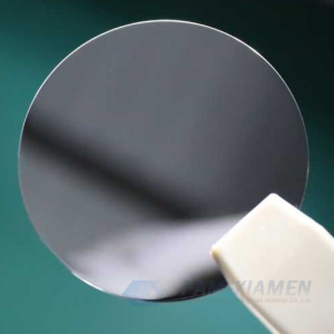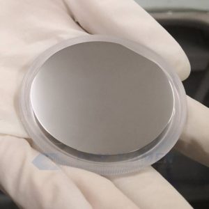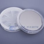
Wafer GaSb
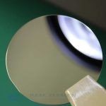
Gallium antimonide (GaSb) material from Ganwafer a gallium antimonide wafer supplier is an important substrate material for manufacturing 2~4um lasers, infrared light-emitting tubes and high-speed low-noise avalanche photodiodes. Its three- and quaternary compound epitaxial growth has good lattice matching, and it is one of the ideal light source materials for manufacturing optical communication devices. Device manufacturing on single crystal GaSb substrate requires the preparation of a stable oxide layer with low interface density, high resistivity, high breakdown voltage and suitable for high-temperature processes. More about GaSb (Gallium Antimonide) crystal substrates please contact us.
- Penerangan
- Siasatan
Penerangan
As one of important III–V compound semiconductor materials, gallium antimonide is applied in optoelectronic devices. Because of the gallium antimonide properties, such as high quantum efficiency, high hole mobility, and super lattices with customized optical and transport characteristics, devices fabricated on GaSb substrate is ideal for the mid-infrared (2-5um and 8-14um wavelength) applications, like imaging sensors for fire detection, surveillance system and environmental pollution monitors.
1. Spesifikasi Wafer GaSb 4″ Epitaxy-ready
| Perkara | Spesifikasi | ||
| Dopant | doped rendah | Zink | Telurium |
| Jenis pengaliran | Jenis-P | Jenis-P | N-jenis |
| Diameter Wafer | 4 " | ||
| wafer Orientation | (100) ± 0.5 ° | ||
| Ketebalan Wafer | 800±25um | ||
| Negara Flat utama | 32.5±2.5mm | ||
| Menengah Flat Negara | 18±1mm | ||
| Konsentrasi Pembawa | (1-2)x1017cm-3 | (5-100)x1017cm-3 | (1-20)x1017cm-3 |
| Mobility | 600-700cm2/vs | 200-500cm2/vs | 2000-3500cm2/vs |
| EPD | <2×103cm-2 | ||
| TTV | <15um | ||
| BOW | <15um | ||
| WARP | <20um | ||
| Penandaan laser | atas permintaan | ||
| Kemasan permukaan | P/E, P/P | ||
| Epi bersedia | yes | ||
| Pakej | bekas wafer tunggal atau kaset | ||
2. Spesifikasi Wafer Gallium Antimonide 3″
| Perkara | Spesifikasi | ||
| Jenis pengaliran | Jenis-P | Jenis-P | N-jenis |
| Dopant | doped rendah | Zink | Telurium |
| Diameter Wafer | 3 " | ||
| wafer Orientation | (100) ± 0.5 ° | ||
| Ketebalan Wafer | 600±25um | ||
| Negara Flat utama | 22 ± 2mm | ||
| Menengah Flat Negara | 11±1mm | ||
| Konsentrasi Pembawa | (1-2)x1017cm-3 | (5-100)x1017cm-3 | (1-20)x1017cm-3 |
| Mobility | 600-700cm2/vs | 200-500cm2/vs | 2000-3500cm2/vs |
| EPD | <2×103cm-2 | ||
| TTV | <12um | ||
| BOW | <12um | ||
| WARP | <15um | ||
| Penandaan laser | atas permintaan | ||
| Kemasan permukaan | P/E, P/P | ||
| Epi bersedia | yes | ||
| Pakej | bekas wafer tunggal atau kaset | ||
3. 2″ Spesifikasi Substrat Wafer GaSb (Gallium Antimonide).
| Perkara | Spesifikasi | ||
| Dopant | doped rendah | Zink | Telurium |
| Jenis pengaliran | Jenis-P | Jenis-P | N-jenis |
| Diameter Wafer | 2 " | ||
| wafer Orientation | (100) ± 0.5 ° | ||
| Ketebalan Wafer | 500±25um | ||
| Negara Flat utama | 16±2mm | ||
| Menengah Flat Negara | 8±1mm | ||
| Konsentrasi Pembawa | (1-2)x1017cm-3 | (5-100)x1017cm-3 | (1-20)x1017cm-3 |
| Mobility | 600-700cm2/vs | 200-500cm2/vs | 2000-3500cm2/vs |
| EPD | <2×103cm-2 | ||
| TTV | <10 pagi | ||
| BOW | <10 pagi | ||
| WARP | <12um | ||
| laser Marking | atas permintaan | ||
| kemasan permukaan | P/E, P/P | ||
| Epi Sedia | yes | ||
| Pakej | bekas wafer tunggal atau kaset | ||
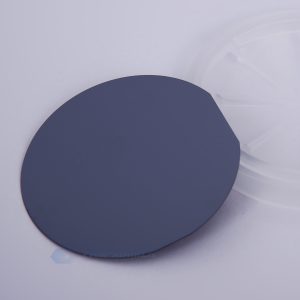
Banyak ciri peranti semikonduktor berkait rapat dengan ciri-ciri permukaan semikonduktor. Perlu diingat bahawa wafer GaSb kristal tunggal mudah dioksida oleh oksigen atmosfera yang membentuk oksida permukaan semula jadi dengan ketebalan beberapa nanometer kerana ia mempunyai permukaan reaktif kimia yang sangat tinggi.
Catatan:
Kerajaan China telah mengumumkan had baharu untuk pengeksportan bahan Gallium (seperti GaAs, GaN, Ga2O3, GaP, InGaAs dan GaSb) dan bahan Germanium yang digunakan untuk membuat cip semikonduktor. Mulai 1 Ogos 2023 dan seterusnya, mengeksport bahan ini hanya dibenarkan jika kami mendapat lesen daripada Kementerian Perdagangan China. Harap untuk pemahaman anda!