GaInP/AlInP発光ダイオード構造
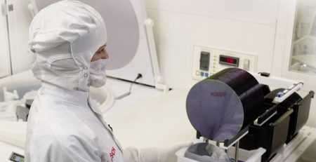
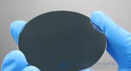
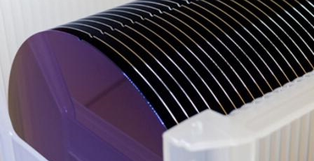
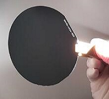
Light emitting diode (LED) structure with GaInP / AlInP epilayers can be offered by Ganwafer. The ternary InGaP and AlInP materials are lattice matched to GaAs susbtrate, which can be grown by MOCVD. Growing high quality III-V三元半導体材料 is important to the fabrication of light emitting diodes, laser diodes and multi-junction photovoltaic. Light emitting diode structure with ternary GaInP and AlInP epilayers from Ganwafer is shown as follows:
1.発光ダイオードのGaAsエピ構造
No.1 GaAs LED Epitaxy
|
GaAs LED Structure (GANWP20065-LED) |
||
| レイヤー素材 | 厚さ | 注意 |
| p-GaInP | – | Composition of In: 0.5;
Mgをドープしました |
| p型GaPの | – | |
| p-AlInP | – | |
| MQW | – | |
| n-AlInP | – | |
| DBR | – | |
| エッチングストップn-GaInP | 20 nm | |
| バッファ層 | – | |
| GaAs潜水艦。 | 350 um | |
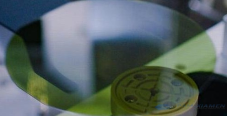
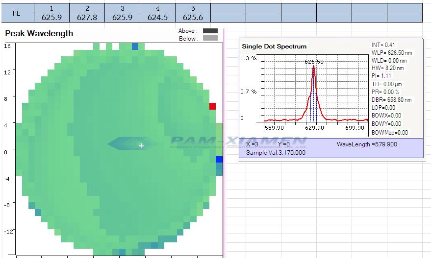
量子発光ダイオードウェーハのPLおよびElテストを図に示します。
No. 2 GaAs based InGaP LED Epitaxy Wafer
GANW190724-INGAP
| Layer Name | 材料 | 厚さ |
| P-cladding layer | P-AlInP | – |
| アクティブレイヤー | MQW | – |
| N-cladding layer | N-AlInP | 900nm |
| Bragg reflector | N-AlGaAs/AlAs | – |
| バッファ層 | N-GaAs | |
| 基板 | N-GaAs on-axis (100) plane without offcut |
No. 3 GaAs based LED Epitaxial Structure
GANWP19168-INGAP
| Layer Name | 材料 | 厚さ |
| P-cladding layer | P-AlInP | – |
| アクティブレイヤー | MQW | – |
| N-cladding layer | N-AlInP | – |
| バッファ層 | N-GaAs | 300nm |
| 基板 | N-GaAs on-axis (100) plane without offcut |
2. FAQ of GaAs Light Emitting Diode Wafer
Q:We observed two MQW regions in GaInP LED wafer (GANWP19168-INGAP), illustrated in below figure. There are 9 pairs in each MQW separated by a thick barrier layer. May I know any reason to grow this kind of structure instead of a single stack of MQWs?
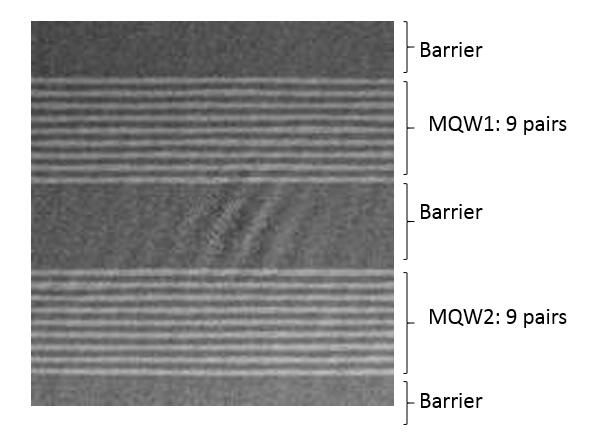
A: These are two groups of identical quantum wells in InGaP LED epitaxy. In order to increase the thickness of the active region and improve the reliability of the LED chip, the middle layer can be used normally without any influence on the photoelectric performance.
3. InGaP on GaAs for Light Emitting Diode Structure
アルミニウム含有材料の代替として大きな可能性を示すInGaPは、通常GaAs基板上に成長する重要な半導体材料です。 その特性は、成長方法、基板温度、成長速度、基板配向、III / V比などの成長条件と密接に関連しています。したがって、InGaPは、赤色高輝度LEDなどのいくつかのアプリケーションのヘテロ構造の成長に最適です。
InGaP / GaAsヘテロ構造の魅力は、そのバンドアライメントに由来し、原子価バンドオフセット(AEv = 0.24 – 0.40 eV)は、伝導バンドオフセット(Mc = 0.03 – 0.22 eV)よりも大幅に大きくなります。 これは、AlGaAs/GaAsヘテロシステムのバンド構造よりも有利であると考えられています。
InGaPは、LEDのエピタキシャル構造のエッチング停止層として使用されるGaAsへの高度に選択的なエッチングです。 これにより、マイクロ発光ダイオードデバイスの成形性と製造性が向上します。 しかし、GaInPエッチング停止層は、電子がコレクターからサブコレクターに流れるときに克服しなければならないエネルギー障壁の高さを増加させます。 この状態では、MQWLED構造のDC電流ゲインが低下します。 したがって、InGaPのエッチング停止層は、デバイスのパフォーマンスを確保するために十分に薄くする必要があります。
詳細については、メールでお問い合わせください。 sales@ganwafer.com と tech@ganwafer.com.