ウェーハファウンドリサービス
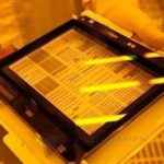
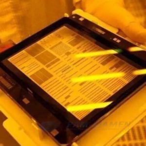
Semiconductor foundry service according to customer demand designs and manufactures wafer from small quantity into production. Wafer foundry services of Ganwafer are offered for micro-electrical mechanical systems (MEMS), power electronics, sensors, microprocessors and etc. Our semiconductor foundry business is all over the world for electronic equipment manufacturers, research institutions, universities and so on. Semiconductor foundry process of Ganwafer includes chemical mechanical polishing (CMP), physical vapor deposition (PVD), chemical vapor deposition (CVD), screen printing, dry etching, wet etching, photolithography, wafer-scale packaging, and other processes.
- 説明
- 問い合わせ
説明
半導体ファウンドリプロセスは、生ウェーハから半導体チップまでのプロセスです。 従来のウェーハファウンドリサービスとは、ウェーハ上に製造されるトランジスタ、抵抗器、その他の電子部品の処理ステップを指します。
1.半導体ファウンドリサービス
当社の半導体ファウンドリは、お客様にフルサービスを提供します。
–MEMS二次元材料統合サービス。
–ポリイミドプロセス;
–ウェーハエッチングプロセス。
–コーティングプロセス;
–フォトリソグラフィープロセス;
–ウェーハボンディングなど。
2.半導体ファウンドリ容量
| プロセス名 | ウェーハサイズ(インチ) | 能力 |
| ステッパーフォトリソグラフィー | 6 | 0.40um |
| 接触したフォトリソグラフィー | 2,4 | 3um |
| ドライエッチング | 6 | 深さ100um(Si)、金属、GaN |
| ウェットベンチ | 6,8 | 金属、SiO2、SiN、TEOS、ポリシリコン |
| PECVD | 6 | SiN SiO2.TEOS |
| LPCVD | 6 | SiN、SiO2。ポリシリコン |
| ALD | 6 | Al2O3, AIN |
| 燻る | 6 | Ti, Al, TiN, Ni, W, TiW, WN |
| Eビーム | 4,6,8 | Ti, Ni, Ag, Al, Ta,Cr, Pt, Mo, Co |
| 移植 | 6 | B(20- 200KeV,1E13-1E15), N |
| RTP | 6 | 最大900℃ |
| オーブン | 6 | 最大400℃ |
また、半導体ファウンドリ企業の1つとして、MEMS、GaAsなどの半導体デバイスのシングルステップおよびマルチステップの製造サービスを提供しています。当社は高度なマイクロナノ設計技術を有しており、世界レベルに達しています。 また、半導体ファウンドリのほぼすべての種類のウェーハは、さまざまなアプリケーションでの製造デバイスに対する顧客の要求を満たすことができます。