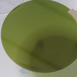
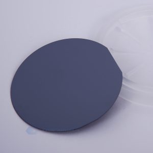
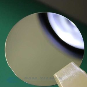
Ganwafer offers semiconductor wafer materials, including compound semiconductor wafer (such as GaSb, InAs, and InSb wafer), Germanium (Ge) wafer, and CdZnTe (CZT) wafer.
半導体ウェーハについて
半導体ウェーハは通常、集積回路を作るための電子機器で広く使用されている半導体物質の薄膜です。 半導体エピウェーハは、私たちが使用するすべての電子機器にASICまたはICとして存在します。
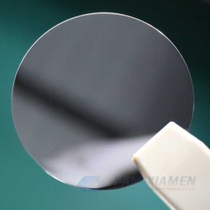
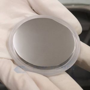
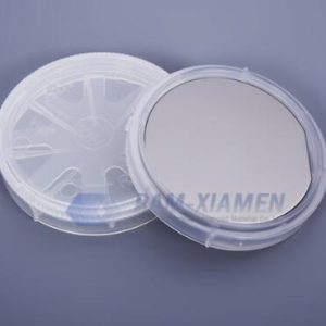
Semiconductor substrate and wafer are a round piece of wafer that consists of the wafer die that performs a very specific functionally. They are the basic material for manufacturing electronic chips. The basic semiconductor substrate wafer manufacturing process includes wafer growth, wafer cleaning and wafer packaging.
Ganwafer is one of a leading semiconductor wafer manufacturing companies that offers a wide range of wafers in different sizes in this case diameters. The semiconductor wafer size has increased throughout to reduce production costs in our semiconductor wafer foundry.
The thickness of semiconductor wafers can vary greatly. The thickness of a wafer is determined by the mechanical strength of any material used to make it. No matter how a wafer is made, the wafer layers must be thick enough to support its own weight so as not to break during processing.