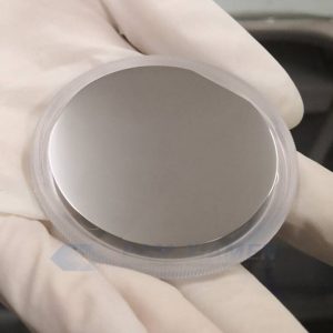
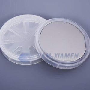
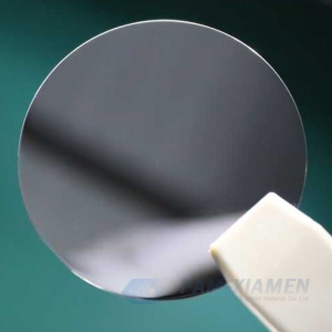
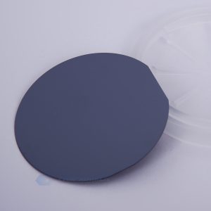
Compound semiconductor materials, like GaAs compound, GaSb compound, InAs compound, InSb compound, InP compound, are provided with high electron mobility.
Compound semiconductor is compounds formed by two or more elements in a definite atomic ratio, and have certain semiconductor properties such as a forbidden band width and an energy band structure. The industry chain can be divided into wafer preparation, chip design, chip manufacturing, and chip packaging and testing. Wafer preparation is further subdivided into two parts: compound semiconductor substrate preparation and compound semiconductor epitaxial wafer preparation.
有機金属気相成長法(MOVPE)は、化合物半導体ファウンドリがデバイス用の化合物半導体薄膜を形成するための最も一般的な手法です。 さらに、MBE、HVPE、LPE、MOMBE、ALDなどの技術を使用して、化合物半導体材料を成長させることができます。
現在、ALD技術の成熟に伴い、化合物半導体n型、p型、半絶縁性型のHMET構造やMOSFET構造に基づくデバイスの品質と信頼性が大幅に向上し、化合物半導体の占有率がさらに向上しています。高周波および高電圧アプリケーションの分野における材料市場。
Regarding compound semiconductor applications, the semi-conductors are mainly used in following fields:
オプトエレクトロニクスデバイス:化合物半導体基板の主なオプトエレクトロニクスアプリケーションには、太陽電池、半導体照明、レーザー、検出器などがあります。
マイクロ波無線周波数:複合半導体ウェーハの主な用途は、無線周波数パワーアンプです。
パワーデバイス:複合ウェーハは主に高電圧スイッチングデバイスで使用されます。 従来のSiプロセスデバイスと比較して、化合物半導体デバイスは、より高い電力密度、より低いエネルギー損失、およびより優れた高温安定性を備えています。
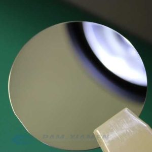
化合物半導体
Copyright◎2021 ガンウエハーファー All Right Reserved