シリコンウェーハ上での薄膜堆積と金属化
Ganwafer, a metal deposition manufacturing company, offers metal film deposition services on silicon by various metal thin film deposition techniques, such as evaporating, sputtering, LPCVD, ALD and etc. All the metal deposition on silicon wafer is supplied at different stress level with high thickness uniformity. The metal deposition process forms contacts in doped area between the semiconductor and conducting path. For our metal deposition service, we use metal and ITO (indium tin oxides) material to prepare electrodes for silicon substrate, and use non-metallic materials to grow sacrificial and insulating dielectric layers on silicon substrate.
- 説明
- 問い合わせ
説明
During the metal deposition process, there are several requirements crucial for integrated microelectronic devices, which should be followed:
The purity of metal should be as high as enough;
It is possible to integrate stacked layers;
The current carrying capacity should be high;
The contact resistance between metal and semiconductor should be low;
The metalizing process should be simple;
The material for metallization should be corrosion-resistant and has a long life;
The material for deposition should be excellent adhesion on silicon oxides.
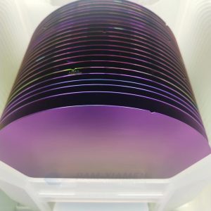
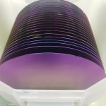
Take the following technical parameters of our deposition metal silicon wafer as an example:
1. Technical Parameters of Metal Deposition on Semiconductor
| 4″ Si Substrate + SiO2 + TiO2 + Pt | ||
| アイテム | パラメータ | |
| 材料 | 単結晶シリコン | |
| グレード | プライムグレード | |
| 成長方法 | CZ | |
| 直径 | 100.0±0.3mm、4インチ | 100±0.3mm、4インチ |
| 導電型 | Nタイプ | Nタイプ |
| ドーパント | リン | ドープされていない |
| 方向付け | <100>±0.5° | [111]±0.5° |
| 厚さ | 300±25μm(全厚) | 525±25μm |
| 抵抗率 | 1-10Ωcm | N / A |
| プライマリフラット | SEMISTDフラット | SEMISTDフラット |
| セカンダリフラット | SEMISTDフラット | SEMISTDフラット |
| 表面仕上げ | 片面研磨 | |
| エッジが丸みを帯びている | SEMI標準ごとに丸められたエッジ | |
| Si Sub / SiO2 / TiO2 / Pt | 総厚300μm Si基板の厚さ289μm 第1中間層SiO2の厚さ10,000オングストローム 第2中間層Tiの厚さ500オングストローム トップレイヤーPt5000オングストローム |
Si基板の厚さ525μm 第1中間層SiO2の厚さ300オングストローム 第2中間層Tiの厚さ20オングストローム トップレイヤーPtオングストローム |
| 粒子 | SEMI STD | |
| TTV | <10um | |
| ボウ/ワープ | <30um | |
| TIR | <5µm | |
| 酸素含有量 | <2E16 / cm3 | |
| 炭素含有量 | <2E16 / cm3 | |
| OISF | <50 /cm² | |
| 攪拌(15x15mm) | <1.5µm | |
| MCCライフタイム | N / A | |
| 表面の金属汚染 Fe、Zn、Cu、Ni、K、Cr |
≤5E10原子/ cm2 | |
| 転位密度 | SEMI STD | |
| 欠け、引っかき傷、でこぼこ、かすみ、タッチマーク、オレンジピール、ピット、ひび、汚れ、汚れ | すべてなし | |
| レーザマーク | SEMI STD | |
2.金属蒸着技術
2.1大気圧CVD(APCVD)
APCVDは、ドープまたは非ドープの酸化物堆積のためのCVD法の1つです。 プロセス中の温度が低いため、堆積した酸化物の密度が低く、適度な被覆率が得られます。 金属堆積基板の高出力は、APCVDプロセスの大きな利点です。
2.2低圧CVD(LPCVD)
LPCVD法では、真空が使用されます。 この方法により、窒化ケイ素(Si3N4)、酸窒化ケイ素(SiON)、二酸化ケイ素(SiO2)、タングステン薄膜をシリコン基板上に堆積させることができ、高い適合性を備えた金属化ウェーハが得られます。
2.3原子層堆積(ALD)
ALDは、Si基板上に金属薄膜を蒸着するのに適した改良されたCVDプロセスです。 ALDを使用すると、3D構造を非常に均一に堆積できます。 絶縁膜と導電性膜の両方を異なる基板(半導体、ポリマーなど)で成長させることができます。