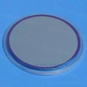
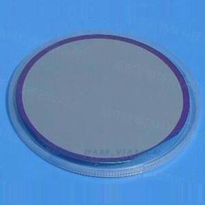
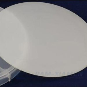
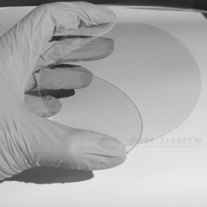
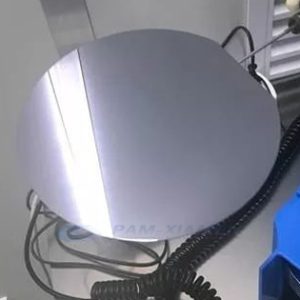
Ganwafer offers N-type, P-type, and semi-insulating gallium nitride substrate, template and gallium nitride epitaxial wafer for HEMT with low marco defect density and dislocation density.
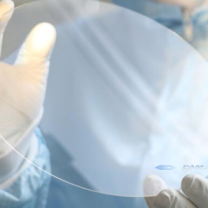
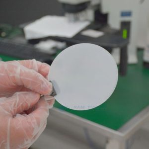
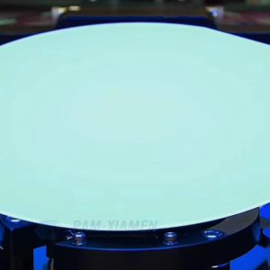
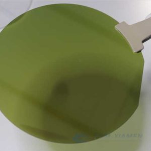
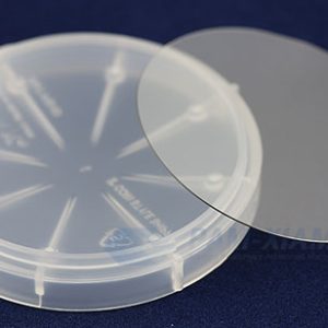
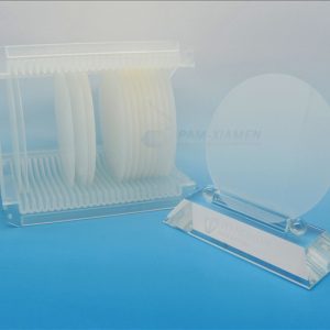
Ganwafer is a leading gallium nitride semiconductor manufacturer that offers wafers in different thicknesses and orientations with polished or unpolished sides and can comprise dopants. Gallium nitride is a wideband gap material that provides higher efficiency and power density than conventional semiconductors at the device level. The benefits include converting into size reduction, less power consumption, and affordable cost.
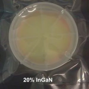
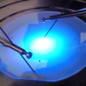
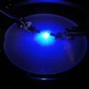
エピタキシャル技術の出現により、シリコンウェーハ、サファイアウェーハ、またはSiCウェーハ上の窒化ガリウムは、エピタキシーによって成長した複雑な多層構造になっています。 窒化ガリウム薄膜は、LED、LD、その他の用途など、優れた性能を発揮する電子デバイスの製造に広く使用されています。 当社の製品は、自立型GaN基板、サファイア/ SiC /シリコン上のGaNテンプレート、サファイア/ SiC /シリコン上のGaNHEMTから、GaNベースのLEDエピタキシャルウェーハにまで及びます。
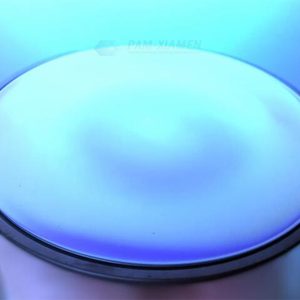
液相平衡系から結晶化したGaNウェーハは、転位の少ない優れた結晶性を示します。 これらの窒化ガリウムウェーハを使用して製造されたさまざまな製品の出力と効率。
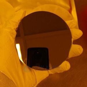
不純物含有量が少ないため、GaNウェーハは、光吸収係数が低く、透過性が高く、出力の向上に役立ちます。
窒化ガリウムウェーハ市場では、クライアントの仕様に関心があります。 また、商用および研究用アプリケーションのカスタムアレンジメントと新しい独自のテクノロジーについても説明します。 信頼性の高い窒化ガリウムウェーハサプライヤーとして、当社は標準的なカスタムパッケージを提供しています。 詳細については、お問い合わせください。