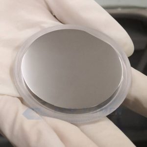
GaSbウェーハ
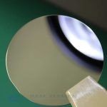
Gallium antimonide (GaSb) material from Ganwafer a gallium antimonide wafer supplier is an important substrate material for manufacturing 2~4um lasers, infrared light-emitting tubes and high-speed low-noise avalanche photodiodes. Its three- and quaternary compound epitaxial growth has good lattice matching, and it is one of the ideal light source materials for manufacturing optical communication devices. Device manufacturing on single crystal GaSb substrate requires the preparation of a stable oxide layer with low interface density, high resistivity, high breakdown voltage and suitable for high-temperature processes. More about GaSb (Gallium Antimonide) crystal substrates please contact us.
- 説明
- 問い合わせ
説明
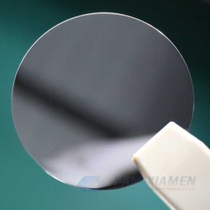
As one of important III–V compound semiconductor materials, gallium antimonide is applied in optoelectronic devices. Because of the gallium antimonide properties, such as high quantum efficiency, high hole mobility, and super lattices with customized optical and transport characteristics, devices fabricated on GaSb substrate is ideal for the mid-infrared (2-5um and 8-14um wavelength) applications, like imaging sensors for fire detection, surveillance system and environmental pollution monitors.
1.4インチエピタキシー対応GaSbウェーハ仕様
| アイテム | 仕様書 | ||
| ドーパント | 低ドープ | 亜鉛 | テルル |
| 伝導型 | P型 | P型 | N型 |
| ウェーハの大口径 | 4 " | ||
| ウエハオリエンテーション | (100)が0.5°、±します | ||
| ウェーハ厚さ | 800±25um | ||
| プライマリフラット長 | 32.5±2.5mm | ||
| セカンダリフラット長 | 18±1mm | ||
| キャリア濃度 | (1-2)x1017cm-3 | (5-100)x1017cm-3 | (1-20)x1017cm-3 |
| モビリティ | 600-700cm2 / Vs | 200-500cm2 / Vs | 2000-3500cm2 / Vs |
| EPD | <2×103cm-2 | ||
| TTV | <15um | ||
| 弓 | <15um | ||
| ワープ | <20um | ||
| レーザーマーキング | 要求に応じて | ||
| 表面仕上げ | P / E、P / P | ||
| エピ準備 | はい | ||
| パッケージ | シングルウェーハコンテナまたはカセット | ||
2.3インチアンチモン化ガリウムウェーハの仕様
| アイテム | 仕様書 | ||
| 伝導型 | P型 | P型 | N型 |
| ドーパント | 低ドープ | 亜鉛 | テルル |
| ウェーハの大口径 | 3 " | ||
| ウエハオリエンテーション | (100)が0.5°、±します | ||
| ウェーハ厚さ | 600±25um | ||
| プライマリフラット長 | 22±2mm | ||
| セカンダリフラット長 | 11±1mm | ||
| キャリア濃度 | (1-2)x1017cm-3 | (5-100)x1017cm-3 | (1-20)x1017cm-3 |
| モビリティ | 600-700cm2 / Vs | 200-500cm2 / Vs | 2000-3500cm2 / Vs |
| EPD | <2×103cm-2 | ||
| TTV | <12um | ||
| 弓 | <12um | ||
| ワープ | <15um | ||
| レーザーマーキング | 要求に応じて | ||
| 表面仕上げ | P / E、P / P | ||
| エピ準備 | はい | ||
| パッケージ | シングルウェーハコンテナまたはカセット | ||
3. 2インチGaSb(アンチモン化ガリウム)ウェーハ基板の仕様
| アイテム | 仕様書 | ||
| ドーパント | 低ドープ | 亜鉛 | テルル |
| 伝導型 | P型 | P型 | N型 |
| ウェーハの大口径 | 2 " | ||
| ウエハオリエンテーション | (100)が0.5°、±します | ||
| ウェーハ厚さ | 500±25um | ||
| プライマリフラット長 | 16±2mm | ||
| セカンダリフラット長 | 8±1mm | ||
| キャリア濃度 | (1-2)x1017cm-3 | (5-100)x1017cm-3 | (1-20)x1017cm-3 |
| モビリティ | 600-700cm2 / Vs | 200-500cm2 / Vs | 2000-3500cm2 / Vs |
| EPD | <2×103cm-2 | ||
| TTV | <10um | ||
| 弓 | <10um | ||
| ワープ | <12um | ||
| レーザーマーキング | 要求に応じて | ||
| 表面仕上げ | P / E、P / P | ||
| エピレディー | はい | ||
| パッケージ | シングルウェーハコンテナまたはカセット | ||
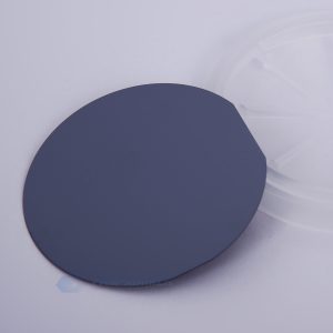
多くの半導体デバイスの特性は、半導体表面の特性と密接に関連しています。 単結晶GaSbウェーハは、化学反応性の高い表面を持っているため、大気中の酸素で形成された数ナノメートルの厚さの自然表面酸化物によって酸化されやすいことは注目に値します。
述べる:
中国政府は、半導体チップの製造に使用されるガリウム材料(GaAs、GaN、Ga2O3、GaP、InGaAs、GaSbなど)およびゲルマニウム材料の輸出に対する新たな制限を発表しました。 2023 年 8 月 1 日以降、これらの材料の輸出は中国商務省から許可を取得した場合にのみ許可されます。 ご理解いただければ幸いです。